Embedded system is the heart and core of most electronic products available in the market. It’s the implementation of engineering in which hardware meets the software. We are surrounded by a world of embedded systems, with mini-computers in biometric door locks, airplanes, cars, pacemakers, etc. These resources constrained, small, smart and powerful systems help us in our daily tasks.
Ever gave a thought on how our body is functioning, the nervous systems, brain and ability to multi-task. If you combine all these functions, you would get a rough picture of a biological embedded system. Our brain hides the complex detail of its functioning that takes place inside it but yet allows us to control it to maximum potential. The same complexity goes for the processor or controller used in embedded systems. They hide complex details and provide us a high-level interface to work upon. For the level of abstraction, one can relate how the code for adding two numbers in a high level programming language cause the registers in the chips handle bits and give an output back to the user.
Processor Architectures
The Central processing unit, referring to both microprocessor and microcontroller, performs specific tasks with the help of a Control Unit (CU) and Arithmetic Logical Unit (ALU). As the instructions are delivered from RAM, the CPU acts with the help of its two helping units by creating variables and assigning them values and memory. It’s really important to know how the CPU performs all this action with the help of its architecture. If you want to know more about how a microcontroller works, you can read this basic of microcontroller article.
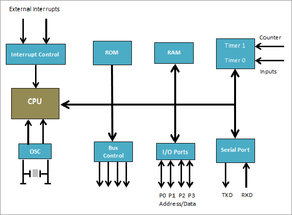
Every CPU has a memory associated with it to store the program and data. Program and data work with the CPU to get the output. The Program provides the instruction while the data provides the information to be worked upon. To access the program and data CPU uses buses, these buses are wires, more precisely these are the wire traces as you may have seen on the printed circuit boards. Over these years microcontrollers and microprocessors have evolved by adapting various architectures, based on the application or design requirements the selection of microcontroller is influenced by the type of architecture used in it. Let’s take a look at the popular architectures.
Von-Neumann /Princeton architecture
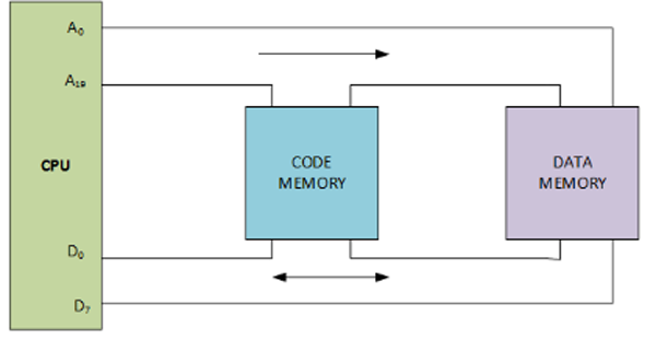
The way by which the CPU gets access to the program and data, tells about the architecture of the CPU. Earlier a single bus was used for getting access to the program and data. This type of architecture is known as the Von Neumann Architecture or more simply Princeton Architecture. A single bus for getting the code and data means, they come to get in each other’s way and slow down the processing speed of the CPU because each had to wait for the other to finish the fetching. This limitation is also known as the Von-Neumann bottleneck condition.
Harvard architecture
To speed up the process Harvard Architecture was proposed. In this architecture a separate data buses for data and program are present. So it means this architecture proposed the use of four buses
- A set of data bus carrying the data into and out of the CPU.
- A set of address bus for accessing the data.
- A set of data bus for carrying code into the CPU.
- An address bus for accessing the code.
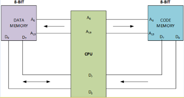
The use of separate address bus and data bus meant low execution time for the CPU but this comes at the cost of complexity in designing the architecture. The Von Neumann architecture may sound a bit lazy but it has the advantage of its simple design.
Harvard architecture is much easy to implement when the CPU and the memory units share the same space or the RAM and ROM are inbuilt (on-chip) with the processing unit, such as in microcontroller where the distances are in microns and millimeters. However, the same architecture is hard to implement where the memory holding the code is external to the processing unit such as that in x86 IBM PC’s. A set of separate wire traces for both the data and address on the motherboard would make the board complex and expensive. Let’s understand it with an example of a processor.
A processor with 64-bit data bus and 32-bit address bus would need approximately 100 buses (96 for the data and address bus and few others for the control signals) for implementation of Von-Neumann architecture. The same structure if implemented with the Harvard architecture would cost the double wire traces approximately 200 with a large number of pins coming out of the processor. It’s for the same reason we don’t see pure Harvard architecture implemented for PC’s and workstations. Instead, a modified Harvard architecture is used in which memory hierarchy with CPU cache memory is used for separating the program and data. Memory hierarchy separates the storage based on the hierarchy of the response time of the processes.
Instruction Set Architecture
As the program (code) is loaded into the memory of the system (RAM) it is fetched by the CPU (referring both microprocessor and microcontroller) to act on the data, it is much similar as we give instructions when we train the dog for certain actions and commands. As those instructions are acted upon certain transistors goes from one logic level to another to make that happen. So basically with the help of instructions human programmer communicates with the processor. Every CPU has its own instruction set, a collection of instructions based on its architecture and capabilities.
CPU understands these instructions in the combination of 0’s and 1 are which are also known as an opcode. For a human programmer, it’s really difficult to remember the combination of 0’s and 1’s for every instruction that is associated with the CPU. To keep the job of a human programmer easy, we are provided with high-level interfaces of these instructions and the compiler converts them in the form of 0’s and 1’s for its processing. Also in the instruction set of each CPU, it has a limited number of instructions that it can understand.
Performance of CPU
You may have heard the term clock rate of CPU related to the performance of the CPU. CPU’s generally have a clock rate in MHz (Mega-Hertz) or GHz(Giga-Hertz) like 25 GHz clock rate. The number associated with the clock rate tells how many times the clock inside the CPU ticks in cycles per second. The practicality of the clock rate can be understood by the fact that instructions are performed based on clock cycles of the CPU which is proportional to the number of programs CPU can run at a time.
The performance of the CPU depends upon the number of instructions that are written in the program, more the instructions, more the time taken by CPU to perform them. It also depends on the number of clock cycles in which each instruction is executed, certain instructions need more clock cycles to be executed than others so they lag the performance of the CPU. Instructions in a program and cycles required to perform each instruction are inversely proportional to each other. Changing one will affect the other. This is the point where the CPU industry is divided.
RISC and CISC Instruction Set Architecture
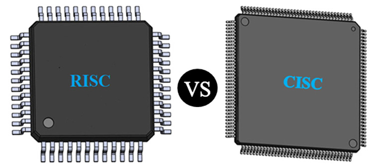
As said above the Execution of a program and the performance of the CPU depends upon the number of instructions in a program wherein the instructions are proposed to that particular CPU as a part of the instruction set and the second factor is the number of clock cycles in which each instruction is executed. Based upon these two factors there is currently two instruction set available. The earliest of which is Complex Instruction Set Computing (CISC) while the other one is Reduced Instruction Set Computing (RISC). Let’s discuss each of these architecture in detail to understand the difference between RIC and CISC Architecture.
Complex Instruction Set Computing (CISC)
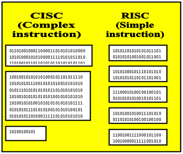
CISC stands for Complex Instruction Set Computing. The main motive of CISC is to reduce the number of instructions that a program executes, this is done by combining many simple instructions like address mode, loading, etc. and to form a single complex instruction. The CISC instruction includes a series of simple instruction as well as some special instructions that takes more than one clock cycle to execute. The CISC instructions can directly work upon memory without the intervention of registers which means it eliminates the need for some basic instructions like loading of values and the requirement of memory (RAM). CISC instructions emphasize more on hardware than on the software, which means that instead of putting the load on the compilers, CISC uses transistors as the hardware to decode and implement instructions. However, as instruction is complex and constitutes of multiple steps, they are executed in more number of clock cycles.
A simple analogy to relate is when you are told to open the book and read the 3rd chapter’s 2nd page. In this series of activities, you do multiple steps like finding the book from your bag than shuffling the page to chapter 3 and then going to the 2nd page of the chapter and then start reading. The series of a step if combined in a single instruction of reading page 44 (which is the 2nd page number of 3rd chapter), we get a CISC instruction.
Reduced Instruction Set Computing (RISC)
The first integrated chip was designed by Jack Kilby in 1958 which was an oscillator and in 1970’s first commercial Microprocessor came out from Intel. Although at the starting of the processors there was no CISC. But with the heavy computing demands CISC architecture was becoming more complex and hard to handle. A total redesign of CISC architecture known as RISC came out from IBM by John Coke. Thus to differentiate between the two architectures the terms RISC and CISC were introduced.
RISC stands for reduced instruction set computing. The main motive of RISC was to introduce uniformity in the size and execution of instructions. This was done by introducing simple instruction set which could be executed as one instruction per cycle, this is done by breaking complex instruction like of loading and storing into different instruction, where each instruction approximately takes one clock cycle to execute. The RISC architecture includes simple instructions of the same size which could be executed in a single clock cycle. RISC based machines need more RAM than CISC to hold the values as it loads each instruction into registers. Execution of single instruction per cycle gives RISC based machines advantage of pipelining (pipelining is the process in which next instruction is loaded before the first instruction is executed, this increases the efficiency of execution). RISC architecture emphasizes more on the software than on the hardware and requires one to write more efficient software’s (compilers, codes) with fewer instructions. The implementation of RISC may sound a lot hard because of multiple instructions but it is justified by the size of instruction and the fact that each instruction is executed in a single clock cycle.
A simple analogy to understand when one has to perform each step for reading the book by finding the book and then finding the page and then chapter and finally start reading.
Comparing RISC vs CISC Architecture
When we compare RISC and CISC, there’s no winner between RISC and CISC architecture, it all depends upon the application and scenario of use. RISC emphasizes efficiency by taking into account cycles per instructions whereas CISC emphasizes efficiency by the number of instructions in a program. For a better efficiency CISC depends on a few lines of code while the RISC reduces the execution time for each instruction. Fairly, it’s not possible to compare microcontrollers and microprocessors based on these two architectures on common ground.

Taking an example of an instruction for multiplying two 8-bit numbers, a CISC based processor would approximately take 70-80 clock cycles, whereas a RISC based processor would approximately take 30-40 clock cycles, which makes it 2 times faster than CISC. Also, as the CISC based CPU’s needs more clock cycles for execution pipelining of instruction is a much harder task as compared to a single cycle processing in RISC based CPU’s.
Where are CISC and RISC Architectures being used?
At the dawn of processors and controllers, only CISC architecture was present, even though the official name CISC was not there. But with the introduction of software such as compilers, RISC based architecture was set to development. Intel from the starting was dependent on CISC architecture. A few companies which were willing to take the risk on RISC were Apple, Atmel, etc. After few years CISC became a little obsolete and unpopular because of difficulty in improvement. However, Intel never left the CISC and continued its development for the improvements.
Presently, the difference between RISC and CISC architecture is very thin. ARM devices, Atmel’s AVR based devices like Arduino, PICs and almost all smartphone manufacturers use RISC architecture as they are much faster and are less resource consuming and more power-efficient. Purely CISC based devices are still in existence in the Intel x86 series and 8051 controllers. Manufacturer’s like AMD uses a hybrid of RISC and CISC from their 5th generation K5 series. On an Application basis, CISC is preferred for automation devices while the RISC is preferred for video and image processing devices.


