While designing a PCB, there are a lot of instances where we need to dissipate heat from certain components (Linear voltage regulator for example). In most cases, those devices are generic through-hole components, thus heat sinks effectively distribute the heat inside the area of Aluminium and keep the device in cooler ambient conditions. But if we are talking about any SMD device, Heatsinks are not available and most of the time, we have to use copper pouring technology to create an adequate heatsink on the copper layers. Now, this is maybe an effective solution but not as effective as the Aluminium heatsink that is used separately as a component in the PCB.
There are two choices left with the designer:
- Use as much copper as available inside the board.
- Use a separate Heatsink to compensate for the additional heat dissipation.
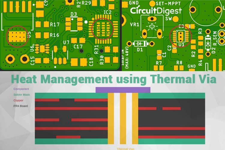
When there is a possibility, many designers will choose the first option as it is much more cost-effective (If designed carefully and additional PCB space will not affect the size of the PCB) and does not affect the manufacturing process as Aluminium heatsinks require screw, heat sealant which is additional manufacturing effort. Now, space-limited PCBs could use two layers, both top, and bottom, and join the two layers to distribute the heat and could be used as a wider area of copper. We are all familiar with the Vias. Vias are the connected holes in the PCB that connect the different copper layers with one and other. These same Vias can be placed just under a surface-mounted device’s heat pad, which allows the heat transfer from the top layer to bottom layers or other layers as well if it is a multi-layer board. These are called Thermal Vias that are situated on the components pad that could reduce thermal dissipation.
Previously, we have discussed different types of vias in PCB that you can use in a PCB design. If you are interested in more PCB design guide articles, you can also check out the article on PCB Power Supply Design Guidelines.
Placement of Thermal Vias
The placements and size of thermal Vias differ largely and it is dependent on the type of components, different rules, and expertise.

But one major rule is to use thermal Vias as close as possible to the heating source directly below the heated components. However, where heat dissipation is not satisfactory, irrespective of component pad placements, thermal Vias can also be placed on the periphery of the component. In this case, the rule also remains the same, that is placing the Vias as close as possible to the periphery of the component.
Thermal Conductivity of Different Material
Thermal conductivity is a key element that is used to determine how much heat can be absorbed by the material. The table below gives you an idea of the thermal conductivity of different materials. With the help of this table, we can make a rule on how we need to manage the Vias.
See the table below:
|
Material |
Thermal Conductivity (W/mK) |
|
Copper |
388 |
|
Lead Frame |
277 |
|
Aluminium |
205 |
|
Silicon |
145 |
|
SnAgCu Solder |
57.3 |
|
63Sn37Pb Material |
50 |
|
DA Epoxy (Die Attach Epoxy) |
2.4 |
|
Mold Compound |
0.7 |
|
FR4 PCB |
0.35 |
Thus, from the above table, it is known that aluminum has a poor thermal conductivity than copper. But, since the Aluminum heatsink gets much more area and it creates a much more effective cooling effect on the heated devices. But, as we can see, if copper is used effectively, it could dissipate much more heat than the same area of aluminum.
An effective thermal via placement is when the Vias are used properly in the IC or the heated components pad that uses conduction, as a heat transfer method, and the heat is distributed among multiple layers of copper and then by the free air, the heat dissipation starts to get transferred on the air using the convection method. It is recommended that the thermal Vias inner diameter need to be smaller, for example - approximately 0.35 mm. If the hole diameter is larger, soldering problems may happen where solder suction will not be proper during the reflow soldering process, so due caution is necessary. However, if a higher diameter is required, thermal padding could be useful to compensate for this.
Key Points to Remember while Placing Thermal Vias
Few things are important to note down during thermal via designing.
1. Exposed pads are designed in such a way that the heat will directly transfer the heat from the case to the copper region. The effect of solder as the heatsink is not significant as it is thin, and the conduction property of solder is poor.

The above image shows thermal Vias on the exposed pad of U1.
2. For exposed pad packages, the maximum heat dissipation happens through the Vias to the bottom layer of the PCB, and then it is dissipated to the air. Thus, having a large area of the bottom layer will also decrease the heat dissipation across the component package.
3. Separating heated components and distributing heat using thermal Vias are helpful to evenly distribute the heat on other packages.
4. Thermal Vias are the only source to dissipate the heat on DFN, QFN packages as the top copper do not have maximum space due to pin allocations. Thus, to use the bottom layer copper, the only way to increase the heat conductivity is to use the Thermal Vias.

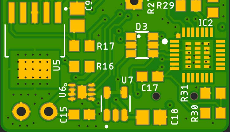
The U5 and IC2 using Thermal vias. IC2 using a QFN flat package where thermal Vias are the only possibility as this does not include a larger copper area on the soldering layer due to the distribution of the component pads.
5. The effective copper area for a thermal via connected device will be the maximum copper length that is directly connected with the component packages using the Thermal via (irrespective of the soldered layer).
6. The thickness of the copper plane is also responsible for the thermal conductivity. 2Oz copper provides better heat resistance than the 1.0 Oz or 0.5Oz copper.
So, this is the standard practice to use Thermal Vias. Hope this article will help many during the design process and placement of the devices that require careful thermal considerations. Please share feedback by using the forum and let us know how efficiently thermal resistance can be improved using different techniques of the Thermal via placements.


