If you have been into PCB design and manufacturing for a long time, you would have probably come across some unexpected problems during the fabrication/manufacturing process. One among those problems is misaligned holes which will make the tracks of your PCB separate over time. By including teardrops in PCB, you can increase the overall quality and stability of the PCB, in the manufacturing process. In this article, we will look into more information about teardrops in PCB. Teardrops are typically drop-shaped vias or junctions that improve the stability of the PCB by providing some margin of redundancy for the via.
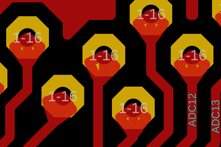
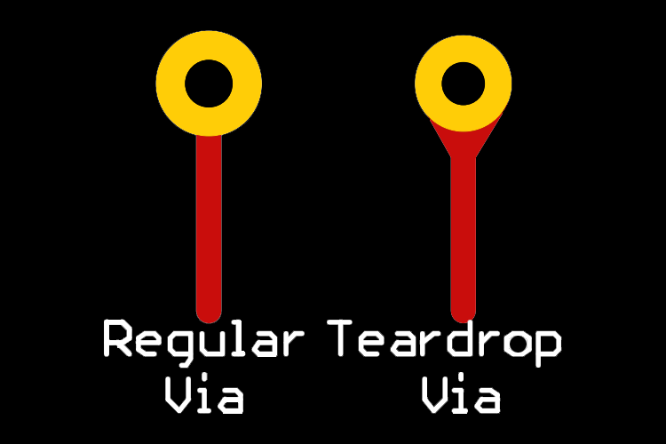
As you can see in the above image, a teardrop is some extra coper at the junction of the pad and trace. It's placed exactly where the trace transitions between thick and thin. If you are doing micro design for the first time, in the PCB industry, it’s a common practice to add teardrops to add some extra redundancy on a circuit board.

So, in this article, we will try to provide sufficient information in which cover all you need to know about teardrops in PCB and how teardrops help to improve the stability of a PCB. We will also know how it's manufactured, and the problems that come along with it. Finally, we will show you how you resolve those problems by using some easily accessible tools that are available in the PCB design software. So without further ado, let’s get right into it.
In many of our previous articles, we have used PCBs to build various projects, you can check those out if you are interested in the topic. You can also check out our article on the basics of PCB if you are new to PCB design.
What is a Teardrop in PCB?
When I heard the term teardrop the first time. My initial reaction was teardrops? IN PCB? What is that? My co-worker told me to do a Google search and learn about it. At that time there was not much content available on the internet so I had to look quite a bit before I understood what teardrops mean.

In the above picture, you can see the clear difference between a teardrop via and a regular via. The waged shape you see on the right-hand side of the image somewhat resembles a teardrop, hence a teardrop via, but in the grand scheme of things, why do we need such a teardrop? If you have this question in mind, follow along and you will have the answer.

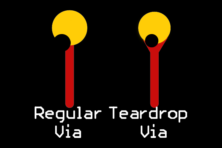
As you can see in the above image, there is a huge mistake by the manufacturer, because while manufacturing the total yield, there will surely be mistakes. Sometimes the drill gets wobbly, sometimes there can be issues with the lamination process, and more. Though manufacturers try to do their best, mistakes often happen and that can reduce the overall product quality. And if a mistake happens, you could end up with a hole created outside the pad or via.
Adding teardrops along the design process is a method to safeguard against drill breakouts because it marginally increases the amount of copper outside the pad. If the drill hole is on the opposite side of the trace, it does not matter much because the connection on the track is still good but if the drill is in the junction in between the trace and the pad, it can cause a serious problem in the long run.
So, the next question would be, how thick or thin should the teardrop be? If you check out your manufacturer’s guidelines, you can find it there but as a general rule of thumb we use:
Apex Radius Factor = ((Diameter of the PAD - Diameter of the Hole)/1.8)
While doing a large PCB design, this gives us a general idea of how the teardrop setting will be.
Adding Teardrops in Your Design
Different manufacturers have their different testing and checking processes, you always need to follow your manufactures guidelines before ordering your PCBs. Often, they will add teardrops as required but it’s a good practice to add your own teardrops in case, the manufacturing house does not provide such advanced features. You need to keep in mind that a trace width of more than 0.5 mm does not require teardrops.
Adding teardrops in eagle:
As you can see in the above example, we are using Eagle PCB designing software to design our PCB, so the options and settings we are using are only applicable to Eagle PCB.
To make teardrops in Eagle, you need to open the ULP from the above ULP menu icon, then search for teardrops, once located you need to double click on it to open it. You just need to put in the radius of the teardrop and click OK. You can calculate the radius of the teardrop by using the formula shown above. Once the teardrops are added, do a proper DRC and ERC check to make sure that no teardrop vias are touching together.
So that’s it for this tutorial. I hope you liked the article and learned something new. If you have any questions regarding the article, please do comment below.


