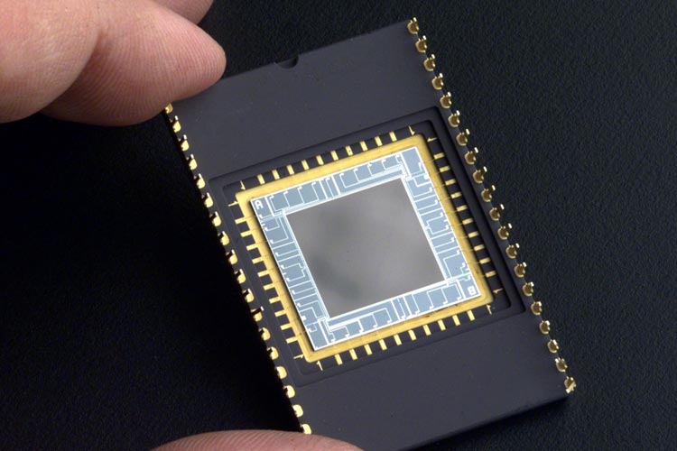
The 60s and 70s were years filled with brilliant discoveries, inventions, and advancements in technology, especially memory technologies. One of the key discoveries at the time was made by Willard Boyle and George Smith, as they explored the application of the metal–oxide–semiconductor (MOS) technology for the development of a semiconductor “bubble” memory.
The team discovered that an electrical charge could be stored on a tiny MOS Capacitor, which could be connected in such a way that the charge could be stepped along from one capacitor to the other. This discovery led to the invention of charge-coupled devices (CCD), which were originally designed to serve memory applications, but have now become important components of advanced imaging systems.
A CCD (Charge Coupled Devices) is a highly sensitive photon detector used in moving charges from within a device to an area where it can be interpreted or processed as information (e.g conversion into a digital value).
In today’s article, we will examine how CCDs work, the applications in which they are deployed, and their comparative advantages to other technologies.
What is a Charge-Coupled Device?
In simple terms, charge controlled devices can be defined as integrated circuits containing an array of linked or coupled, charge storage elements (capacitive bins), designed in such a way that under the control of an external circuit, the electric charge stored in each capacitor can be moved to a neighboring capacitor. Metal-Oxide-Semiconductor capacitors (MOS capacitors) are typically used in CCDs, and by applying an external voltage to the top plates of the MOS structure, charges (electrons (e-) or holes (h+)) can be stored in the resulting potential. These charges can then be shifted from one capacitor to another by digital pulses applied to the top plates (gates) and can be transferred row by row to a serial output register.
Working of Charge-Coupled Device
There are three stages involved in the operation of a CCD and since the most popular application in recent times is Imaging, It is best to explain these stages in relation to imaging. The three stages include;
- Charge Induction/Collection
- Charge Clocking out
- Charge Measurement
Charge Induction/Collection/Storage:
As mentioned above, CCDs are made up of charge storage elements and the type of storage element and method of charge induction/deposition depends on the application. In Imaging, the CCD is made up of a large number of light-sensitive materials divided into small areas (pixels) and are used to build up an image of the scene of interest. When light thrown at the scene is reflected on the CCD, a photon of light that falls within the area defined by one of the pixels will be converted into one (or more) electrons, the number of which is directly proportional to the intensity of the scene at each pixel, such that when the CCD is clocked out, the number of electrons in each pixel is measured and the scene can be reconstructed.
The figure below shows a very simplified cross-section through a CCD.
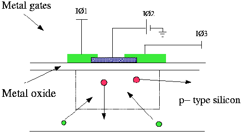
From the image above, it can be seen that the pixels are defined by the position of electrodes above the CCD. Such that if a positive voltage is applied to the electrode, the positive potential will attract all of the negatively charged electrons close to the area under the electrode. In addition, any positively charged holes will be repulsed from the area around the electrode and this will lead to the development of a "potential well" where all the electrons produced by incoming photons will be stored.
As more light falls on the CCD, the “potential well” becomes stronger and attracts more electrons until the “full well capacity” (the number of electrons that can be stored under a pixel) is attained. To ensure that a proper image is captured, a shutter for instance is used in cameras to control the lighting in a timed manner so that the potential well is filled but its capacity is not exceeded as that could be counterproductive.
Charge Clocking Out:
The MOS topology used in CCD fabrication limits the amount of signal conditioning and processing that can be done on-chip. Thus, charges usually need to be clocked out to an external conditioning circuit where processing is done.
Each pixel in a row of a CCD is typically fitted with 3 electrodes as illustrated in the image given below:
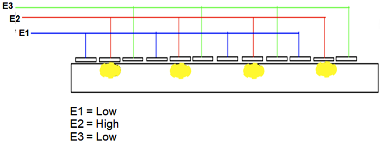
One of the electrodes is used in the creation of the potential well for charge storage while the other two are used in the clocking out of charges.
Say a charge is collected under one of the electrodes as illustrated in the image below:
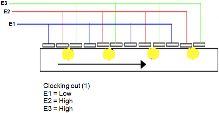
To clock the charge out of the CCD, a new potential well is induced by holding IØ3 high, which forces the charge to be shared between IØ2 and IØ3 as illustrated in the image below.
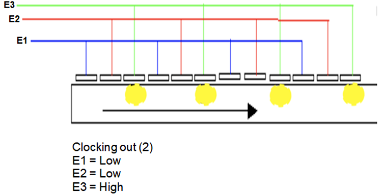
Next, IØ2 is taken low, and this leads to a full transfer of the charge to the electrode IØ3.
The clocking out process continues by taking IØ1 high, which ensures the charge is shared between IØ1 and IØ3, and finally taking IØ3 low so the charge is shifted fully under the IØ1 electrodes.
Depending on the arrangement/orientation of electrodes in the CCD, this process will continue and the charge will move either down the column or across the row till it reaches the final row, usually referred to as the readout register.
Charge Measurement:
At the end of the readout register, a connected amplifier circuit is used to measure the value of each charge and converts it into a voltage with a typical conversion factor of around 5-10µV per electron. In imaging applications, a CCD-based camera will come with the CCD chip along with some other associated electronics but most importantly the amplifier, which by converting the charge into voltage helps to digitize the pixels to a form that can be processed by the software, to obtain the image captured.
Properties of CCD
Some of the properties used in describing the performance/quality/grade of CCDs are:
1. Quantum Efficiency:
Quantum efficiency refers to the efficiency with which a CCD acquires/stores a charge.
In Imaging, not all the photons falling on the pixel planes are detected and converted into an electrical charge. The percentage of photos that are successfully detected and converted is known as Quantum Efficiency. The best CCDs can achieve a QE of around 80%. For context, the quantum efficiency of the human eye is around 20%.
2. Wavelength Range:
CCDs typically have a wide wavelength range, from about 400 nm (blue) to about 1050 nm (Infra-red) with a peak sensitivity at around 700 nm. However, processes like back thinning can be used to extend the wavelength range of a CCD.
3. Dynamic Range:
The dynamic range of a CCD refers to the minimum and the maximum number of electrons that can be stored in the potential well. In typical CCDs, the maximum number of electrons is usually around 150,000, while the minimum may actually be less than one electron in most settings. The concept of dynamic range may be better explained in imaging terms. Like we mentioned earlier, when light falls on a CCD, the photons are converted into electrons and are sucked into the potential well which at some point becomes saturated. The amount of electrons resulting from the conversion of photons typically depends on the intensity of the sources, as such, dynamic range is also used to describe the range between the brightest and faintest possible source that can be imaged by a CCD.
4. Linearity:
An important consideration in the selection of CCD is usually its ability to respond linearly over a wide range of Input. In imaging, for example, if a CCD detects 100 photons and converts the same to 100 electrons (for example, assuming QE is 100%), then for linearity sake, it is expected to generate 10000 electrons if it detects 10000 photons. The value of linearity in CCDs is in the reduced complexity of the processing techniques used in weighing and amplifying the signals. If the CCD is linear, a lesser amount of signal conditioning is required.
5. Power:
Depending on the application, power is an important consideration for any device, and using a low-power component is usually a smart decision. This is one of the things CCDs bring to applications. While the circuitry around them may consume a significant amount of power, CCDs themselves are low power, with typical consumption values around 50 mW.
6. Noise:
CCDs like all analog devices are susceptible to noise, as such, one of the major properties for the evaluation of their performance and capacity is how they deal with noise. The ultimate noise element experienced in CCD is the Readout noise. It is a product of the electrons to the voltage conversion process and is a contributing factor to the estimation of the dynamic range of the CCD.
Applications of CCDs
Charge-coupled devices find applications across different fields including;
1. Life Sciences:
CCD based detectors and cameras are used in diverse imaging applications and systems in life sciences and the medical field. The applications in this area are too vast to mention every single one, but some specific examples include the ability to take images of cells with contrasting enhancements applied, the ability to collect image samples which have been doped with fluorophores (which cause the sample to fluoresce) and use in advanced X-ray tomography systems to image bone structures and soft tissue samples.
2. Optical Microscopy:
While the applications under life sciences include use in microscopes, it is important to note that the microscopy applications are not limited to the life science field. Optical microscopes of diverse types are used in other cogent fields like; nanotechnology engineering, food science, and chemistry.
In most microscopy applications, CCDs are used because of the low noise ratio, high sensitivity, high spatial resolution, and rapid sample imaging which is important for analyzing reactions occurring on microscopic levels.
3. Astronomy:
With microscopy, CCDs are used to image tiny elements but in Astronomy, it is used in focusing the images of large and far away objects. Astronomy is one of the earliest applications of CCDs and objects ranging from stars, planets, meteors, etc. have all been imaged with CCD-based systems.
4. Commercial Cameras:
Low-cost CCD Image sensors are used in commercial cameras. The CCDs are usually of lower quality and performance compared to the ones used in Astronomy and life sciences due to the low-cost requirements for commercial cameras.


