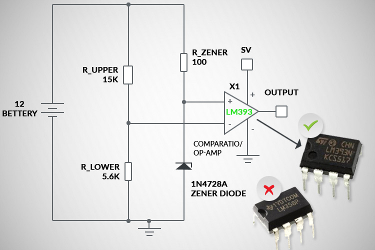
In practical electronic circuits, signal processing is an important constraint and different types of methodologies are required to satisfy the customer demand of various design requirements. For any of the signal conditioning requirements, the Op-Amp is the first choice for any designer to comply with the design requirements and in most cases, the Operation amplifiers will satisfy the requirements as expected. But, why do we use Operational Amplifiers as Comparator?
There are some dedicated devices or components to perform the particular operation. Among them, the comparator is a popular application and in most cases, the Op-Amp circuits are preferred over the dedicated comparator because of any one of the following reasons.
Cost Efficient:
In most of the circuits, the Op-Amps are the mandatory component to process the analog signals. So, commonly the multichannel Channel Op-Amps are selected for a particular circuit and some of the channels are used for true Op-Amp requirements and the remaining channels can be used for the Comparator requirements. With this, the single component satisfies both Op-Amp, comparator requirements which prove beneficial in terms of reduction in the size of the PCB, reduction in the cost of extra component and reduction in the inventory of extra component and also can save a decoupling capacitor which is placed between Vcc to Gnd of any Op-Amp or comparator IC.
Uncomplicated Requirements:
In some of the applications like simple LED indications, turn-on/turn-off simple transistors based on threshold limits, DC, and low-frequency signal comparison circuits, the simple Op-Amps are quite sufficient to satisfy these uncomplicated requirements. If some of the unused Op-Amp channels are available in the circuit, then the Circuit designers generally use that unused op-amp and finish the requirements.
Unavailability of Matching Comparator:
There are different types of circuit specifications available depending upon the design. So, the required comparator specifications also varied based on design requirements. But, comparator availability to satisfy every design requirement is lesser whereas the Op-Amp segment has plenty of options with respect to technology, cost, and packaging, etc. So, in most cases, designers need to go with the Op-Amp to satisfy the comparator requirements.
However, replacing Comparator with the Op-Amp is not an easy task. It requires more insights on important Op-amp parameters to match the Comparator Performances with Op-Amps.
This article will provide the details of the impact of Op-Amp, which is used as a comparator with different practical circuit requirements.
Comparator Circuit for Simple DC Voltage Applications
Low Voltage Indicator Circuit - Example:
Consider a Home UPS system that operates with a Single Lead Acid Battery, this system requires a Low Voltage indicator to warn the Customer about the present low voltage condition of the battery. The Voltage level of the Lead-acid battery is 11.7V to 13.5V under open-circuit conditions. So, with margin, the low current buzzer and warning LED should be turned on when the battery voltage level goes below 12V. The selected LED and Buzzer voltage is assumed to be 3V and the operating current is assumed to be 3mA. The Low Voltage Indicator circuit can be implemented using a Comparator, as shown in Figure 1.
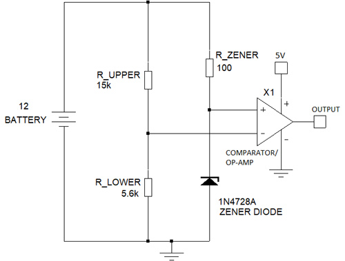
Figure 1: Low Voltage Indicator Circuit using Comparator/Op-Amp
The constant 3.3V reference is applied to the non-inverting comparator pin using Zener Diode. The R_Zener is selected based on the Zener Current value. Based on 1N4728A Datasheet, the Zener Current in this circuit is equal to its test current of 76mA.

Figure 2: Vishay 1N4728A Zener Diode Specifications

The 110.5Ω value is not a standard resistor value. So, 100Ω is selected for R_Zener.
The voltage divider connected to the inverting pin of the comparator provides the Battery Voltage detail and whenever the voltage at inverting pin goes below 3.3V, the LED and Buzzer will be activated by the transistor inside the Comparator.
Comparator Output Configuration:
While selecting a comparator IC for any application, the important parameter to be considered is the Output Configuration of the comparator. The comparators come with two types of output configurations as shown in Figure 3 and the output load of the comparator has to be carefully configured based on the type of comparator output configuration.
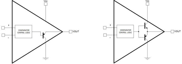
Figure 3: Comparator Output Configurations
For Open Collector Output based configuration, the pull-up resistor should be placed between the Output Pin of the comparator and Source, which energies the output load. It can either be a Comparator Vcc power supply or another power supply. In Push-Pull Configuration, the maximum comparator output voltage will be nearly equal to the Comparator Vcc and the output load is directly connected to the output pin of the comparator.
Output Configuration for different Comparators and Op-Amp:
The below figures show the different output configurations for comparators obtained from the manufacturer datasheets. As per the datasheet, the LM339 has the Open Collector Configuration. So, for the output load, a push-pull resistor and power supply are required.
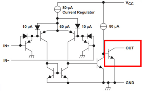
Figure 4: Simplified Schematic of LM339 – Open Collector Output
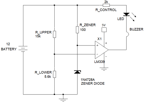
Figure 5: Low Voltage Indicator Circuit using LM339 Comparator
The Low Voltage Indicator Circuit using LM339 Open Collector Output Configuration is shown in Figure 5. Here, the LED and Buzzer are connected with a Pull-up resistor and connected to the comparator output (Open collector) terminal.
The Pull-Up resistor which is used to control the current through Buzzer and LED is selected based on the below calculation. The LED and Buzzer voltage is assumed to be 3V and the operating current is 3mA. LED and Buzzer is connected in series with R_CONTROL resistor and the current in a series circuit is the same which is equal to 3mA.

Meanwhile, the Output configuration of the LMV7239 Comparator shown in Figure 6 has the Push-Pull type output configuration. With LM7239, the output load is directly connected to the output pin of the LM7239. The LM324 Op-Amp internal schematic is shown in Figure 7 and it has the Push-Pull output configuration and all Op-Amps have the Push-Pull Output Configuration only.
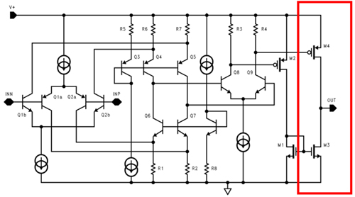
Figure 6: Simplified Schematic of LMV7239 – Push-Pull Output
While connecting directly to the output of the Push-Pull configuration comparator/Op-Amp, the two important points should be taken into consideration.
- The Load Voltage requirement should be less than or equal to the Comparator Output Voltage.
- The Load Current Requirement should be less than the Comparator output current specification.
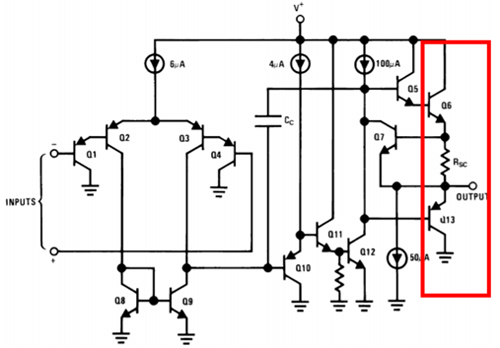
Figure 7: Simplified Schematic of LM324 – Push-Pull Output
Important Parameters to check on Datasheet for Push-Pull Output Configurations
While using Push-Pull Configuration-based comparator and Op-amp, the Output voltage swing is the important parameter that defines how the output load can be connected with the output terminal of the Comparator or Op-Amp.

Figure 8: LMV7239 Output Voltage Swing
From the specification table shown in Figure 8, the maximum output voltage of the output comparator is varied between V+ - 0.25 to V+ - 0.15V (V+ = Vcc = 5V). So, for 5V Vcc, the high rail output voltage varies between 4.75V and 4.85V. The low rail output voltage varies between 230mV to 450mV.
Likewise, the Op-Amp also has the Push-Pull output configuration, and the output voltage swing of LM324 Op-Amp is shown in the Figure given below.

Figure 9: LM324 Output Voltage Swing
As per the LM324 Op-Amp datasheet, the maximum value output voltage is Vcc-1.5 = 5 – 1.5 = 3.5V. So, for 5V Vcc, in any condition, we can’t get more than 3.5V from the Op-Amp output. In the LM7239 comparator, we are getting a maximum of 4.85V for the same 5V Vcc. Whereas, if we search for the High voltage output level in the LM339 comparator, the data will not be available because the output voltage level of LM339 will depend on the supply which is connected to the output transistor
For the implementation of Low voltage indicator with LM7239 Comparator and LM324 Op-Amp, the LED and Buzzer requires 3V individually. So, the series connection of LED and Buzzer will require a total of 6V output and can’t be delivered by both LM7239 and LM324. So, the LED and Buzzer are connected in series and the R_Control resistor value can be calculated as below. The loads are connected in parallel so the total current requirement is 6mA.
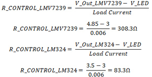
The 308.3Ω and 83.3Ω are not the standard resistor values. So, 300Ω and 82Ω standard values can be selected instead.
The implementation of the Low Voltage indicator circuit with Push-Pull Configuration is shown in Figure 10. In this circuit, the output load voltage requirement is less than the comparator or Op-Amp output voltage level. In case the LED and Buzzer need to be connected in series, then the circuit has to be modifier as shown in Figure 11 with external MOSFET or Vcc that can be increased to a higher voltage level based on Comparator or Op-Amps maximum voltage levels.
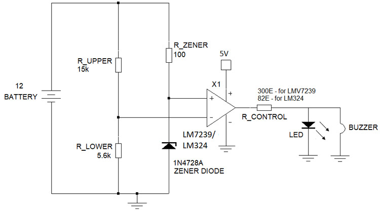
Figure 10: Low Voltage Indicator Circuit using LM7239 Comparator (Load Voltage/Current Requirement lesser than Comparator Output Voltage/Current Specifications)
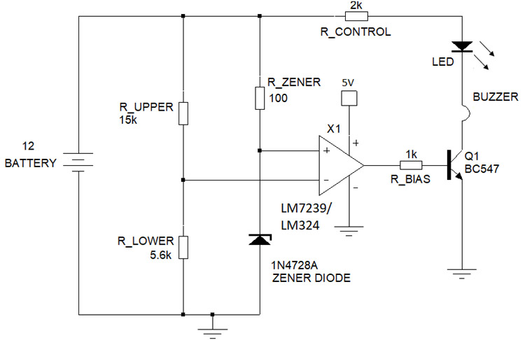
Figure 11: Low Voltage Indicator Circuit using LM7239 Comparator (Load Voltage/Current Requirement higher than Comparator Output Voltage/Current Specifications)
Parameters to be considered on Input Pins
Common Mode Voltage:
The important parameter that should be considered at the input pin is the Common Mode voltage of the inverting and non-inverting Pins. In LM324 Op-Amp the Common-Mode Voltage Range is given in the below figure. LM339 also has the same common Mode voltage level and LM7239 accepts up to Vcc+0.1V. As per the datasheet, it is Vcc-1.5 = 5-1.5 = 3.5V. So, at any condition, the input voltage at any pins should not exceed the Common Mode Voltage. As per the above implementations, the Voltage reference by Zener diode at the Non-Inverting terminal is 3.3V and it is under the Limit of 3.5V. At inverting terminal, the voltage obtained from the voltage divider is less than 3.5V when the battery voltage is less than 12.9V. But, from the specification, we can know that the battery voltage is varied between 11.7V to 13.5V and more than 12.9V, the design will exceed the common-mode voltage limit and create problems in circuit operation. To mitigate this issue in LM339 and LM324, there are two possible ways available.
- Vcc of the Comparator or Op-Amp can be increased to the higher voltage level
- Voltage reference at non-inverting pin and voltage divider can be modified based on the Common Mode voltage level. (Here instead of 3.3V reference 2.7V reference and voltage divider values can be modified accordingly).
- Instead of LM339 and LM324, the LMV7239 can be used which has the 5.1V Common Mode voltage range.

Figure 12: Common-Mode Input Voltage Range LM324
Differential Mode Voltage:
While using Op-Amp as a comparator the basic deciding feature is a differential Voltage specification of Op-Amp. The differential voltage is the difference between the Non-Inverting and Inverting pin voltage levels. In most of the comparators, the differential voltage will be equal to the Vcc. But, in Op-Amps, it will vary based on the Op-Amp model. For some of the Op-Amps like LM324 have a differential voltage level equal to the Vcc and other Op-Amps have less than the differential voltage level of less than Vcc.

Figure 13: Differential Mode Input Voltage Range LM324
In some cases, the Op-Amps have bidirectional back-to-back protection diodes at the input terminals of the Op-Amp. In this case, the maximum allowed voltage difference between the input terminals is only around 0.7V. For example, if the Input Voltage reference at Non-Inverting input is 1V, then at inverting pin, the maximum allowed voltage variation is between 0.3V to 1.7V. Lesser than or higher than the mentioned voltage limit, the Op-Amp circuit may misbehave and lead to wrong results. The Differential mode voltage range of LM324 is given in Figure 13 and the allowed voltage levels are much higher than our requirement.
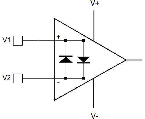
Figure 14: Op-Amp Back to Back diodes at input terminals – Reducing Differential Voltage Specification
Output Current Rating and Temperature Considerations:
In Push-Pull output configuration, the entire load current is supplied via the Op-Amps or the comparators. So, the current requirement should be lesser than the Output Current Specification of the Op-Amp or Comparator. Also, with this comparator operation mode, the Op-Amps work under saturated voltage conditions. So, the increase in load current will also lead to more power dissipation in the Op-Amp and will increase the Op-Amp IC temperature and strict control is required on this part.
Conclusion
Based on the above data, the replacement of Comparator with Op-Amp is quite an easy task with the careful considerations of different input and output voltage parameters for very simple DC voltage applications. However, in High-Frequency applications, the replacement is not easy and it should consider Op-Amp frequency responses, Slew Rate, and propagation delay parameters, and replacing it without detailed analysis will lead to complete design failure.


