Power is an important part of any electronics project/device. Irrespective of the source, there is usually a need to perform power management tasks like voltage transformation/scaling, and conversion (AC-DC / DC-DC) among others. Choosing the right solution for each of these tasks can be key to the success (or failure) of the product. One of the most common power management tasks in almost all kind of device is DC-DC voltage regulation/scaling. This involves changing the value of DC voltage at the input to a higher or lower value at the output. The components/modules used to achieve these tasks are generally referred to as voltage regulators. They generally have the ability to supply a constant output voltage which is higher or lower than the input voltage and they are commonly used to supply power to components in designs where you have sections at different voltages. They are also used in traditional power supplies.
There are two major types of voltage regulators;
- Linear Regulators
- Switching Regulators
Linear voltage regulators are usually step down regulators and they use impedance control to create a linear reduction of the input voltage at the output. They are usually very cheap but inefficient as a lot of energy is lost to heat during the regulation. Switching regulators on the other hand are capable of either stepping up or down the voltage applied at the input depending on the architecture. They achieve voltage regulation using a on/off switching process of a transistor which controls the voltage available at the regulators output. Compared to linear regulators, Switching regulators are usually more expensive and far more efficient.
For today’s article, we will be focusing on switching regulators and as the title gave away, we will be looking at factors to consider when selecting a switching regulator for a project.
Due to the complexity of other parts of the project (the core functionalities, RF etc), the choice of regulators for power supply is usually one of the actions left till the end of the design process. Today’s article will try to provide the time restricted designer, with tips on what to look for in the specifications of a switching regulator, to determine if it fits your particular use case. Details will also be provided on interpreting the different ways in which different manufacturers present information on parameters like temperature, load etc.
Types of Switching Regulators
There are essentially three types of switching regulators and the factors to put into consideration depends on which of the types is to be used for your application. The three types are ;
- Buck Regulators
- Boost regulators
- Buck Boost Regulators
1. Buck Regulators
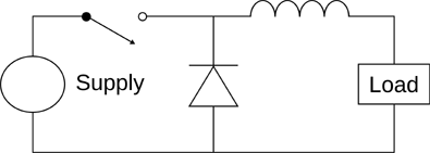
Buck regulators, also called step-down regulators or buck converters are arguably the most popular switching regulators. They have the ability to step-down the voltage applied at the input to a lesser voltage at the output. Thus, their rated input voltage is usually higher than their rated output voltage. A basic schematics for a buck converter is shown below.

The output of the regulator is due to the on and off switching of the transistor and the voltage value is usually a function of the transistor duty cycle (how long the transistor was on in every complete cycle). The Output voltage is given by the equation below from which we can infer that the duty cycle can never be equal to one and thus the output voltage will always be lesser than the input voltage. Buck regulators are therefore used when a reduction in supply voltage is required between one stage of a design and the other. You can learn more about Design basics and efficiency of buck regulator here, further learn how to build a Buck converter circuit.
2. Boost Regulators
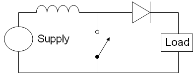
Boost regulators or boost converters operate in a directly opposite manner to the buck regulators. They deliver a voltage higher than the input voltage, at their Output. Like the buck regulators, they use the switching transistor action to increase the voltage at the output and are usually made up of the same components used in buck regulators with the only difference being the arrangement of the components. A simple schematics for the boost regulator is shown below.

You can learn more about Design basics and efficiency of Boost regulator here, can build one Boost converter by following this Boost Converter Circuit.
3. Buck-Boost regulators
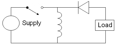
Last but not the least are the buck boost regulators. From their name, it is easy to infer that they provide both the boost and the buck effect to the input voltage. The buck-boost converter produces an inverted (negative) output voltage which can be greater or less than the input voltage based on the duty cycle. The basic buck-boost switch mode power supply circuit is given below.

The buck-boost converter is a variation of the boost converter circuit in which the inverting converter only delivers the energy stored by the inductor, L1, into the load.
The selection of any of these three switching regulator types, depends solely on what is required by the system being designed. Irrespective of the type of regulator to be used, It is important to ensure the specifications of the regulators meets the requirements of the design.
Factors to Consider when Selecting a Switching Regulator
The design of a switching regulator depends in a large measure on the power IC used for it, thus most of the factors to consider will be the specifications of the power IC used. It is important to understand the specifications of Power IC and what they signify so as to ensure you select the right one for your application.
Irrespective of your application, running a check on the following factors will help you reduce the time spent on selection.
1. Input Voltage Range
This refers to tolerable range of input voltages supported by the IC. It is usually specified within the data sheet and as a designer, its important to ensure that the input voltage for your application, falls within the Input Voltage range specified for the IC. While certain data sheets may only specify for the maximum input voltage, it is better to check the data sheet to be sure there is no mention of the minimum input range before making any assumptions. When voltages higher than the max input voltage is applied, the IC’s usually gets fried out but it usually stops operating or operate abnormally when voltages lower than the minimum input voltage is applied, all depending on the protective measures in place. One of the protective measures usually applied to prevent damage to ICs when out of range voltages are supplied at the input is the Under-Voltage Lock Out (UVLO), checking if this is available may also help your design decisions.
2. Output Voltage Range
Switching regulators usually have variable outputs. The output voltage range represents the range of voltages to which your required output voltage can be set. In ICs without variable output option, this is usually a single value. It is important to ensure that your required output voltage is within the range specified for the IC and with a good factor of safety as difference between the maximum output voltage range and the output voltage you require. as a general rule the minimum output voltage cannot be set to a voltage level lower than the internal reference voltage. Depending on your application (buck or boost), the minimum output range can either be greater than the input voltage(boost) or way lesser than the input voltage(buck).
3. Output Current
This term refers to the current rating for which the IC was designed. It is essentially an indication of how much current the IC can supply at its output. For some ICs, Only the maximum output current is specified as a measure of safety and to help the designer ensure the regulator will be able to deliver the current required for the application. For other ICs, both the minimum and maximum ratings are provided. This could be very useful in planning power management techniques for your application.
In selecting a regulator based on the IC’s output current, it is important to ensure a margin of safety exists between the maximum current required by your application and the maximum output current of the regulator. It is important to ensure the max output current of the regulator is higher than your required output current by at least 10 to 20%, as the IC may generate a high amount of heat when operating at maximum levels continuously and could be damaged by the heat. Also the efficiency of the IC reduces when operating at maximum.
4. Operating Temperature Range
This term refers to the temperature range within which the regulator functions properly. It is defined in terms of either the ambient temperature (Ta) or the junction temperature (Tj). The TJ temperature refers to the highest operating temperature of the transistor, while the ambient temperature refers to the temperature of the environment around the device.
If the Operating temperature range is defined in terms of the ambient temperature, it doesn’t necessarily mean the regulator can be used over the full temperature range. It is important to factor in the factor of safety and also factor in the planned load current and the accompanying heat as the combination of this and the ambient temperature is what makes up the junction temperature which should also not be exceeded. Staying within the operating temperature range is critical to the proper, continuous operation of the regulator as excessive heat could lead to abnormal operation and catastrophic failure of the regulator. It is thus important to pay attention to the ambient heat in the environment which the device will be used and also determine the possible amount of heat that will be generated by the device as a result of the load current before determining if the specified operating temperature range of the regulator works for you. Its important to note that certain regulators could also fail in extremely cold conditions and its worth paying attention to the minimum temperature values if the application will be deployed in cold environment.
5. Switching Frequency
Switching frequency refers to the rate at which the control transistor is turned on and off in a switching regulator. In pulse width modulation based regulators, the frequency is usually fixed while in Pulse Frequency Modulation.
The switching frequency affects the parameters of the regulator like the ripple, the output current, the maximum efficiency, and the response speed. The design for the switching frequency always involve the use of matching inductance values, such that the performance of two similar regulators with different switching frequency will be different. If two similar regulators at different frequencies are considered, it will be discovered that, the maximum current for instance will be low for the regulator operating at a lower frequency compared to that of the regulator at high frequency. Also, parameters like ripple will be high and the response speed of the regulator will be low at low frequency, while the ripple will be low and response speed, high at high frequency.
6. Noise
The switching action associated with switching regulators generates noise and related harmonics which could affect the performance of the overall system, especially in systems with RF components and audio signals. While the noise can be reduced by means of a filter etc., it can really reduce the signal to noise ratio (SNR) in circuits that are sensitive to noise. It is thus important to be sure the amount of noise generated by the regulator won’t affect the overall performance of the system.
7. Efficiency
Efficiency is an important factor to consider in the design of any power solution today. It is essentially the ratio of the output voltage to the input voltage. Theoretically, the efficiency of a switching regulator is hundred percent, but this is not usually true in practice as the resistance of FET switch, diode voltage drop and ESR of both inductor and output capacitor reduces the overall efficiency of the regulator. While most modern regulators offer stability across wide operation range, the efficiency varies with use and for instance is greatly reduced as the current drawn from the output increases.
8. Load Regulation
Load regulation is a measure of the ability of a voltage regulator to maintain a constant voltage at the output irrespective of the changes in the load requirement.
9. Packaging and Size
One of the usual goals during the design of any hardware solution these days is to reduce the size as much as possible. This essentially includes reducing the size of the electronics component and invariably reducing the number of components that make up each section of the device. A Small size power system not only helps reduce the overall size of the project, but it also helps create room to which extra product features can be cramped in. Depending on the goals of your project, ensure the form factor/package size you go with will fit into your space budget. While making selections based on this factor, it is also important to factor in the size of the peripheral components required by the regulator to function. For instance, the use of High frequency ICs permit the use of output capacitors with low capacitance and inductors, resulting in a reduced component size and vice versa.
Identifying all of this and comparing with your design requirements will quickly help you determine which regulator should be crossed of and which should feature in your design.
Do share which factor you think i missed out and any other comments via the comment section.
Till Next time.


