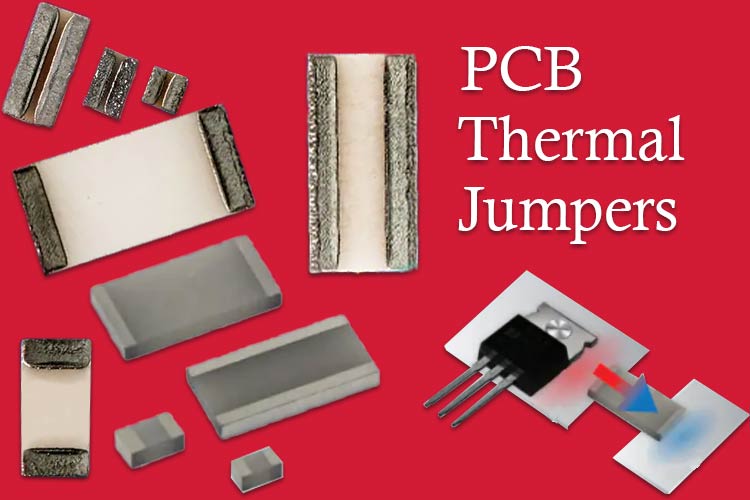
In this article, we will talk about SMD thermal management and design, and specifically about PCB Thermal Jumpers or Thermal Conductors. If we were to take the heat out from a through-hole component, the simple way is to put a big heat sink on and the heat sink will draw out all the heat from the device. The main advantage of the SMD component is that it reduces manual labor, PCBs with SMD parts can directly go to the pick and place and can be soldered autonomously. But when we are talking about thermal heat management things get a little difficult. So in this article, we will talk about different ways to manage heat in your SMD design and how implementing SMD thermal jumpers can impact the thermal performance of the device.
What are SMD Thermal Jumpers and how does it work?
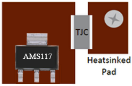
There are many ways to dissipate heat when we are talking about SMD design, the most popular one is to use thermal vias. In some cases to place more than 10 via in one place to dissipate the heat to the ground plane or the VCC plane inside the PCB, this process is called VIA stitching, but in some cases that is not possible. For that, we can take the example of the popular AMS117 IC that puts out the power through the tab connector of the device and that cannot be connected to the ground, this is where SMD Thermal Jumpers comes in, an example is shown below, where an AMS117 device is connected with the PCB and the heat is transferred to the other part of the PCB using a thermal jumper.

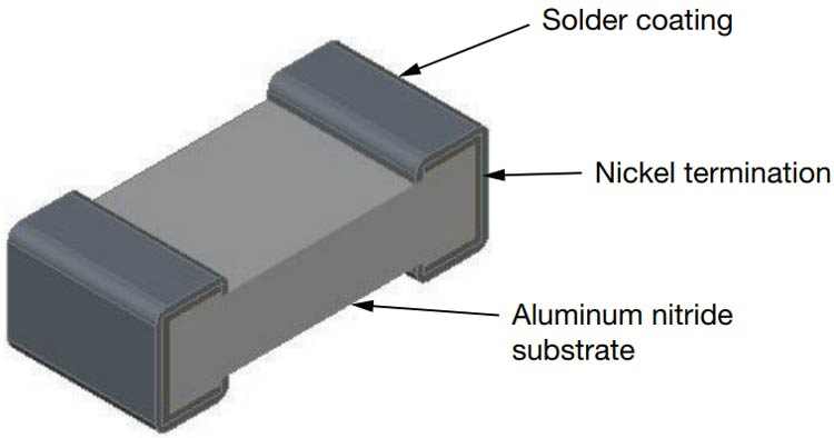
Thermal Jumpers are Surface Mount Chips, designed to provide an electrically isolated thermal conductive pathway to a ground plane or heat sink while maintaining the electrical isolation of the device. The most popular manufacturer is Vishay / Thin Film THJP ThermaWick Thermal Jumper SMD Chips. They are constructed with aluminum nitride substrates in both tin/lead (SnPb) and lead (Pb)-free wraparound termination styles. The low capacitance of THJP Thermal Jumper SMD Chips makes them an excellent choice for high-frequency and thermal-ladder applications.

An image of the actual thermal via is shown above. As you can see in the image above, and it looks very similar to SMD inductors, the difference is that it’s not the two ends of the device are made out of nickel and it has a coating of solder on it. The led and led free version of this device is also available. The main component of this device is the aluminum nitrate substrate, which is responsible for transferring the heat from one surface to another, other than that the resistance of this device is >999M ohms and that’s huge!
The datasheet also provides a pair of thermal images of the device under test, the device is on a standard FR4 PCB substrate with a heat sink pad on the PCB.

The image on the left-hand side shows a ceramic resistor without a thermal jumper and on the right-hand side with a thermal jumper and as you can see the temperature difference is quite huge, 36% overall improvement so to say. At this point, the performance of this device can be improved dramatically, if we implement the VIA stitching method to transfer the heat of the device from one layer to other internal or external layers.

In the above picture, we can see some thermal characteristics, and as you can see the rating that is given is in *C/W that is quite useful for calculations. And if you recall our previous article on PCB thermal, you can understand it is 14*C/W and it's not that great but if we go for the 0612 or 1225 version, you can see the dramatic difference between those two. It drops from 14*C/w to 4*C/W in perspective. It is equivalent to placing 10 thermal via in PCB and it saves huge board space. Also, you can see the capacitance of the device is given which is very useful for high-speed RF design or SMPS design because if you are using this on RF applications capacitance can cause issues. That concludes this article on PCB thermal Jumpers.


