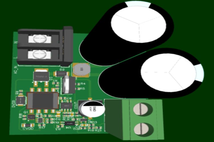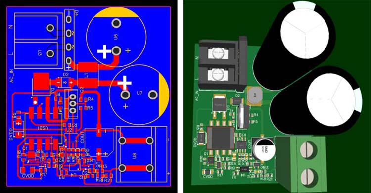
While making a customized RGB LED set up at our home, basically it was a bunch of addressable 5v LEDs the WS2812, but unfortunately, we didn't have a high current power source to light them up properly. Since there was a lot of them, it required around 9 Amps of current to lighten up at full brightness. This led us to design one Power Supply for this purpose, as well as the Gerbers are shared, so if one wants to make this power source they can do so easily.
We have previously built many Power Supply Circuits, check them to learn more about Power Electronics.
What it does?

It is a High Watt Power Supply Unit that converts 85V to 250V RMS AC to 5V DC rated at 60W which provides a current draw of 12 Amps, and that too in a small form factor, and isolated output with high efficiency.
Component Required for AC to DC High Watt Power Supply
Project Used Hardware
- Bridge Rectifier,
- Coupled Transformer,
- CV CC UCC28740 flyback controller by TI,
- UCC24630 Synchronous Rectifier Controller by TI,
- Optocouplers,
- Power Mosfets,
- TL431 adjustable Zener,
- Schottky Diodes,
- Power Inductors,
- Complementary Passive components
Project Used Software
- EasyEDA, TI’s Webench Power Supply Design
Project Hardware Software Selection
First, we tinkered with TI’s Webench Power Supply Design and found some really decent designs, as a perfect match for our requirements. After a while, by getting a balanced result from all ways, i.e a small size, high current draw (12A) ample to source our LEDs, high efficiency; we started making the schematic in EasyEDA. Next, we designed the PCB and rechecked every connection thoroughly for any disputes. Obviously, we don't want to get ourselves zapped. Main Components Used: Bridge Rectifier Coupled Transformer CV CC UCC28740 flyback controller by TI UCC24630 Synchronous Rectifier Controller by TI Optocouplers Power Mosfets TL431 adjustable Zener Schottky Diodes Power Inductors Complementary Passive components Challenges we ran into Orienting the PCB Layout was a bit challenging, Along with that routing and connecting the components was a bit tricky.
Circuit Diagram
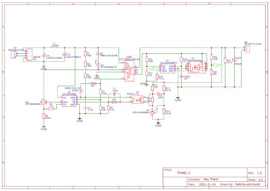
The circuit consists of the following stages: First, the rectifier converts the AC to pulsating DC and after that, it goes through a PI filter that smoothens the pulsating DC to stable DC, then this high voltage DC is chopped by the flyback controller and fed into a transformer that not only steps the voltage down but also provides galvanic isolation. An optocoupler constantly monitors the output voltage and provides feedback to the flyback controller and changes the pulse width for controlling the output voltage. The output is driven through a high power MOSFET with a decent amount of heatsinking capability that can drive high loads.
Accomplishments
Accomplishments that we're proud of: Making the PCB design and completing the project on time with video and presentation was our greatest achievement.
What we learned?
It was a good experience, about learning about the fly-back controller, which not only provides isolation but also has great efficiency. How SMPS has been so efficient and small yet delivering such high power.
What's next for Zeus
Later this week we are thinking of fabricating this PCB along with component sourcing, to make it real.
Warning- This Circuit deals with AC mains (aka High Voltage that can kill you). Take High precautions before performing. You have been warned.


