In the measurement industry, a very crucial functional block is a Programmable Gain Amplifier (PGA). If you are an electronic enthusiast or a college student, you have probably seen a multimeter or oscilloscope measuring very small voltages very preciously because the circuit has a built-in PGA alongside a powerful ADC that helps with the precise measurement process.
Nowadays, off the shelf PGA amplifier offers an op-amp based, a non-inverting amplifier with a user-programmable gain factor. This type of device has very high input impedance, wide bandwidth, and a selectable input voltage reference built into the IC. But all these features come with a cost, and for me, it's not worth putting that costly of a chip for a generic application.
So to overcome these situations, I have come up with an arrangement consisting of an Op-amp, MOSFET, and Arduino, through which I was able to change the gain of the op-amp programmatically. So, in this tutorial, I am going to show you how to build your own Programmable Gain Amplifier with an LM358 op-amp and MOSFETS, and I will be discussing some pros and cons of the circuit alongside testing.
Basics of Op-Amp
To understand the working of this circuit, it is very important to know how an operational amplifier works. Learn more about Op-amp by following this op-amp tester circuit.

In the above figure, you can see an operational-amplifier. The basic job of an amplifier is to amplify an input signal, alongside amplification, the op-amp can also do various operations like sum, differentiate, integrate, etc. Learn more about the summing amplifier and differential amplifier here.
Op-amp has only three terminals. The terminal with the (+) sign is called non-inverting input, and the terminal with the (-) sign is called inverting input. Besides these two terminals, the third terminal is the output terminal.
An op-amp only follows two rules
- No current flows in or out of the op-amp inputs.
- The op-amp tries to keep the inputs at the same voltage levels.
So with those two rules cleared up, we can analyze the below circuits. Also, learn more about Op-amp by going through various Op-amp based circuits.
Programmable Gain Amplifier Working
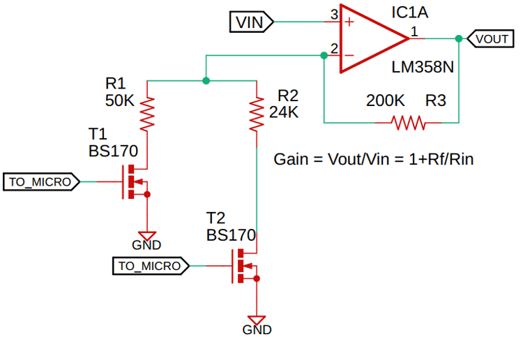
The above figure gives you a basic idea about the circuit arrangement of my crud PGA Amplifier. In this circuit, the op-amp is configured as a non-inverting amplifier, and as we all know with a non-inverting circuit arrangement, we can change the gain of the op-amp by changing the feedback resistor or the input resistor, as you can see from the above circuit arrangement, I just need to switch the MOSFETs one at a time to change the gain of the op-amp.
In the test section, I did just that I switched the MOSFETs one at a time and compared the measured values with the practical values, and you can observe the results in the "testing the circuit" section below.
Components Required
- Arduino Nano - 1
- LM358 IC - 1
- LM7805 regulator - 1
- BC548 Generic NPN Transistor - 2
- BS170 Generic N-channel MOSFET - 2
- 200K Resistor - 1
- 50K Resistor - 2
- 24K Resistor - 2
- 6.8K Resistor - 1
- 1K Resistor - 4
- 4.7K Resistor - 1
- 220R, 1% Resistor - 1
- Tactile Switch Generic - 1
- Amber LED 3mm - 2
- Bread Board Generic - 1
- Jumper Wires Generic - 10
- Power Supply ± 12V - 1
Schematic Diagram
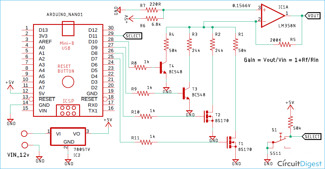
For a demonstration of Programmable Gain Amplifier, the circuit is constructed on a solderless breadboard with the help of the schematic; To reduce internal parasitic inductance and capacitance of the breadboard, all the components have been placed as close as possible.
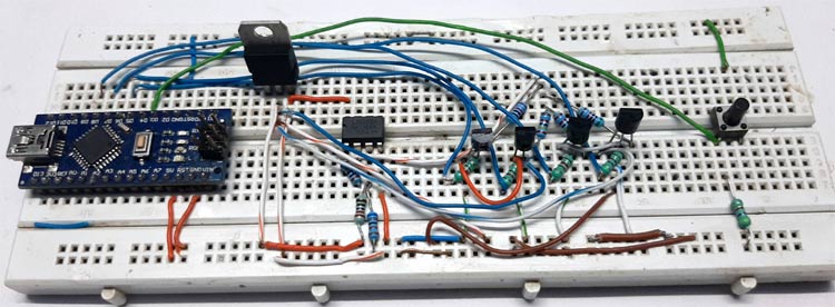
And if you are wondering why there is a cluster of wires in my breadboard? let me tell you it's to make a good ground connection as internal ground connections in a breadboard are very poor.
Here the op-amp in the circuit is configured as a non-inverting amplifier and the input voltage from the 7805 voltage regulator is 4.99V.
The measured value for the resistor R6 is 6.75K and R7 is 220.8R these two resistors form a voltage divider which is used to generate the input test voltage for the op-amp. The Resistors R8 and R9 are used to limit the input base current of the transistor T3 and T4. The resistors R10 and R11 are used to limit the switching speed of the MOSFETs T1 & T2, otherwise, it can cause oscillation in the circuit.
In this blog, I want to show you the reason for using a MOSFET rather than a BJT, hence the circuit arrangement.
Arduino Code for PGA
Here Arduino Nano is used to control the base of the transistor and the gate of the MOSFETs, and a multimeter is used to show the voltage levels because the built-in ADC of the Arduino does a very poor job, when it comes to measure low voltage levels.
Complete Arduino code for this project is given below. As this is a very simple Arduino code we do not need to include any libraries. But we do need to define some constants and input pins as shown in the code.
The void setup() is the main functional block where read and write operation for all the inputs and outputs are performed as per requirement.
#define BS170_WITH_50K_PIN 9
#define BS170_WITH_24K_PIN 8
#define BC548_WITH_24K_PIN 7
#define BC548_WITH_50K_PIN 6
#define BUTTON_PIN 5
#define LED_PIN1 2
#define LED_PIN2 3
#define PRESSED_CONFIDENCE_LEVEL 5000
int button_is_pressed = 0;
int debounce_counter = 0;
void setup() {
  pinMode(BS170_WITH_50K_PIN, OUTPUT);
  pinMode(BS170_WITH_24K_PIN, OUTPUT);
  pinMode(BC548_WITH_24K_PIN, OUTPUT);
  pinMode(BC548_WITH_50K_PIN, OUTPUT);
  pinMode(LED_PIN1, OUTPUT);
  pinMode(LED_PIN2, OUTPUT);
  pinMode(BUTTON_PIN, INPUT);
}
void loop() {
  bool val = digitalRead(BUTTON_PIN);  // read input value
  if (val == LOW) {
    debounce_counter++;
    if (debounce_counter > PRESSED_CONFIDENCE_LEVEL)
    {
      debounce_counter = 0;
      button_is_pressed++;
    }
    if (button_is_pressed == 0) {
      digitalWrite(BS170_WITH_50K_PIN, HIGH);
      digitalWrite(BS170_WITH_24K_PIN, LOW);
      digitalWrite(BC548_WITH_24K_PIN, LOW);
      digitalWrite(BC548_WITH_50K_PIN, LOW);
      digitalWrite(LED_PIN1, LOW);
      digitalWrite(LED_PIN2, LOW);
    }
    if (button_is_pressed == 2) {
      digitalWrite(BS170_WITH_24K_PIN, HIGH);
      digitalWrite(BS170_WITH_50K_PIN, LOW);
      digitalWrite(BC548_WITH_24K_PIN, LOW);
      digitalWrite(BC548_WITH_50K_PIN, LOW);
      digitalWrite(LED_PIN1, LOW);
      digitalWrite(LED_PIN2, HIGH);
    }
    if (button_is_pressed == 3) {
      digitalWrite(BC548_WITH_24K_PIN, HIGH);
      digitalWrite(BC548_WITH_50K_PIN, LOW);
      digitalWrite(BS170_WITH_24K_PIN, LOW);
      digitalWrite(BS170_WITH_50K_PIN, LOW);
      digitalWrite(LED_PIN1, HIGH);
      digitalWrite(LED_PIN2, HIGH);
    }
    if (button_is_pressed == 1)  {
      digitalWrite(BC548_WITH_50K_PIN, HIGH);
      digitalWrite(BS170_WITH_50K_PIN, LOW);
      digitalWrite(BS170_WITH_24K_PIN, LOW);
      digitalWrite(BC548_WITH_24K_PIN, LOW);
      digitalWrite(LED_PIN1, HIGH);
      digitalWrite(LED_PIN2, LOW);
    }
    if (button_is_pressed >= 4) {
      button_is_pressed = 0;
    }
 }
}
Calculations for Programmable Gain Amplifier
The measured values for the PGA amplifier circuit are shown below.
Vin = 4.99V
R7 = 220.8 Ω
R6 = 6.82 KΩ
R5 = 199.5K
R4 = 50.45K
R3 = 23.99K
R2 = 23.98K
R1 = 50.5K
Note! The measured values of the resistor are shown because with measured resistor values we can closely compare the theoretical values and practical values.
Now the calculation from the voltage divider calculator is shown below,

The output of the voltage divider is 0.1564V
Calculating the gain of the non-inverting amplifier for the 4 resistors
Vout when R1 is the selected resistor
Vout = (1+ (199.5 / 50.5) ) * 0.1564 = 0.77425V
Vout when R2 is the selected resistor
Vout = (1+ (199.5 / 23.98) ) * 0.1564 = 1.45755V
Vout when R3 is the selected resistor
Vout = (1+ (199.5 / 23.99) ) * 0.1564 = 1.45701V
Vout when R4 is the selected resistor
Vout = (1+ (199.5 / 50.45) ) * 0.1564 = 0.77486V
I did all that to compare the theoretical and practical values as close as possible.
With all the calculations done, we can move on to the testing section.
Testing of Programmable Gain Amplifier Circuit
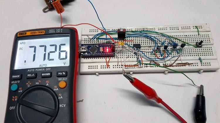
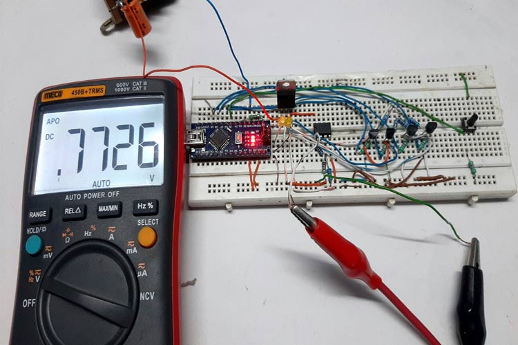
The above image shows you the output voltage when the MOSFET T1 is on, hence current is flowing through the Resistor R1.
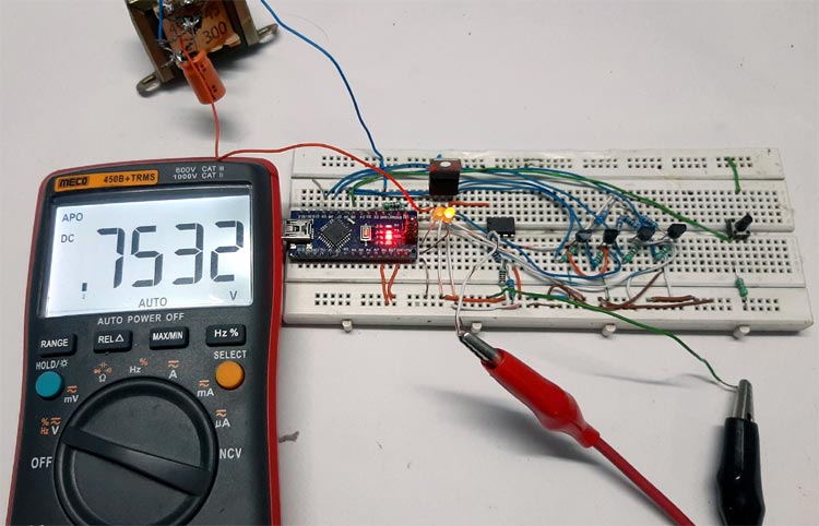
The above image shows you the output voltage when Transistor T4 is on, hence current is flowing through the Resistor R4.
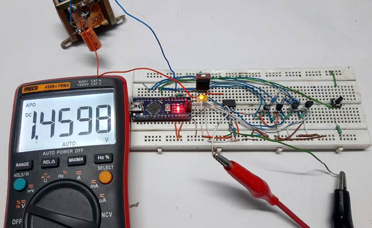
The above image shows you the output voltage when the MOSFET T2 is on, hence current is flowing through the Resistor R2.
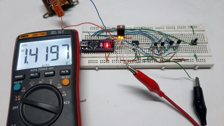
The above image shows you the output voltage when Transistor T3 is on, hence current is flowing through the Resistor R3.
As you can see from the schematic that T1, T2 are MOSFETs, and T3, T4 are transistors. So when MOSFETs are used, the error is in 1 to 5 mV range but when transistors are used as switches we are getting an error in 10 to 50 mV range.
With the above results, it's clear that the MOSFET is the goto solution for this kind of application, and the errors in the theoretical and practical may be caused due to the offset error of the op-amp.
Note! Please note that I have added two LEDs just for the sake of testing and you can't find them in the actual schematic, it shows binary code to show which pin is active
Pros & Cons of Programmable Gain Amplifier
As this circuit is cheap, easy, and simple, it can be implemented in many different applications.
Here MOSFET is used as a switch to pass all the current through the resistor to ground that is why the effect of temperature is not certain, and with my limited tools and test equipment, I was not able to show you the effects of varying temperature on the circuit.
The objective of using a BJT alongside MOSFETs is because I want to show you how poor a BJT can be for this kind of application.
The values of the feedback resistors and the input resistors must be in the KΩ range, that is because with lower resistor values, more current will flow through the MOSFET, thus more voltage will drop across the MOSFET causing unpredictable results.
Further Enhancement
The circuit can be further modified to improve its performance like we can add the filter to reject high-frequency noises.
As LM358 jelly bean op-amp is used in this test, the offset errors of the op-amp are playing a major role at the output voltage. So it can be further improved by using an instrumental amplifier rather than an LM358.
This circuit is made just for demonstration purposes only. If you are thinking about using this circuit in a practical application, you have to use a chopper type op-amp and high precision 0.1 ohms resistor to achieve absolute stability.
I hope you liked this article and learned something new out of it. If you have any doubt, you can ask in the comments below or can use our forums for detailed discussion.

