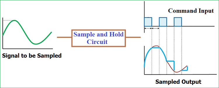
Sample and Hold Circuit takes samples from the analog input signal and hold them for particular period of time and then outputs the sampled part of input signal. This circuit is only useful for sampling few microseconds of input signal.
A Sample and Hold circuit consist of switching devices, capacitor and an operational amplifier. Capacitor is the heart of the Sample and Hold Circuit because it is the one who holds the sampled input signal and provide it at output according to command input. This circuit is mostly used in Analog to Digital Converters to remove certain variations in input signal, which may corrupt conversion process.
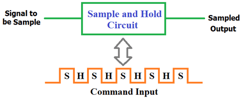
A typical block diagram of Sample and hold circuit is mentioned below:

Generally applied input voltage signal is a continuously changing analog signal. Command input is provided to trigger the sampling and holding of input signal. Command input is nothing but a on/off signal to start/stop sampling of input signal, it is generally PWM. The sampling and holding process is depends upon the command input. When the switch is closed the signal is sampled and when its open the circuit holds the output signal. The On/OFF condition of switch is controlled by command input.
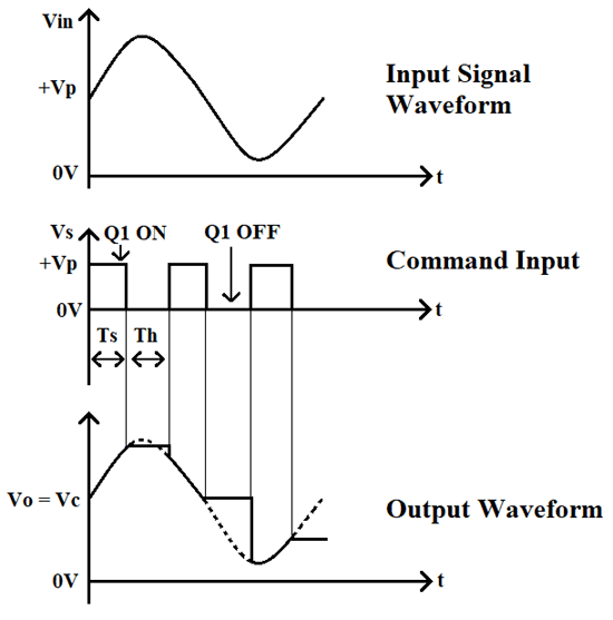
The ideal input and output waveform of the sample and hold circuit is given below:

It can be clearly understood from the above diagram that this circuit takes samples of input signal for the time Command Input is high and replicate the same sample at the output. And when the command input is LOW, it keeps the last voltage level of sampled signal.
If we simulate our Sample and Hold Circuit, we will get the above waveform. The complete sample and hold circuit simulation video is given at the end.
Material Required
- uA741 Op-Amp IC
- 2N4339 N-channel JFET
- Analog Input and Pulse Input Generator
- Resistor (10k, 10M)
- Diode (1N4007)
- Capacitor (0.1uf - 1nos)
Circuit Diagram
For providing analog signal at input terminal you can use 6-0-6 step-down transformer. And, for giving pulse or PWM input to the transistor you can use 555 timer IC in astable mode. We also need a DC supply for the providing Vcc to the Op-amp IC which will be in range of +5 to +15V.
Working of Sample and Hold Circuit
As you can in the circuit diagram, we have used 2N4339 N-channel JFET, an op-amp, and a capacitor. A command input (a PWM input) is connected to the Gate terminal of the 2N4339 transistor. As you can in the circuit diagram, we have used 2N4339 N-channel JFET, an op-amp, and a capacitor. A command input (a PWM input) is connected to the Gate terminal of the 2N4339 transistor. A diode 1N4007 is also connected between command input and 2N4339 N-channel JFET.
Now, the question is why the diode is connected in reverse condition? Let me give you a brief introduction about 2N4339. 2N4339 is an N-channel JFET with low noise and high gain. 2N4339 conducts (turn ON) only when gate-to-source voltage is in range of -0.3v to -50v (max). Now, we have set the initial voltage of command input to -15V and pulsed voltage to 15V. So, whenever the command input voltage is negative the diode will be forward biased which cause the transistor to turns ON and vice versa.
The Op-amp 741 is used as a voltage follower here, because voltage follower generally has a high input impedance and a low output impedance. This is used when the input signal is of low current becuase voltage follower can supply sufficient current to the next stage.
So, whenever the command input is HIGH the transistor works as closed switch and at this moment the capacitor starts charging to its peak value and stores the sample of input signal for the time transistor is in on state. Now when the command input is LOW the transistor works as open switch and the capacitor will experience high impedance and due to this it cannot get discharged and holds the charge for a particular period of time. This time is known as Holding Period. And, the time during which the circuit samples the input signal is called as the Sampling Period.
Some Applications of Sample and Hold Circuit
- ADCs (Analog-to-Digital Conversion)
- DACs (Digital-to-Analog Conversion)
- In Analog Demultiplexing
- In Linear Systems
- In Data Distribution System
- In Digital Voltmeters
- In Signal Constructional Filters


