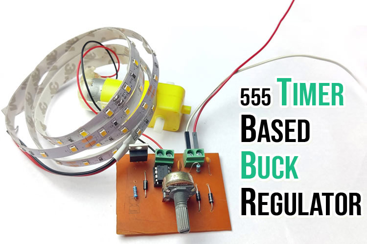
In this article, we will make a buck converter using 555 timer IC and a IRFZ44N N channel MOSFET and use it as LED dimmer circuit or as a motor speed controller circuit. This circuit is basically a simple power electronics DC-DC Buck converter which can be used to step down voltage, its efficiency results in better battery life due to reduced heat generation making it a lucrative option for smaller gadgets. I have designed a converter circuit using KiCAD and fabricated a simple in-house PCB and tested the module with a LED strip.
How is a buck converter different from a linear voltage regulator and why is it more efficient?
Both the buck converters and linear regulators are step down converters, i.e. the output voltage is lower than the input voltage. The buck converters employ PWM switching technique to step down the voltage, whereas the linear regulator acts as a variable resistor constantly maintaining the voltage divider network in order to maintain constant output, but the down side is that they waste the energy in the form of heat to maintain the output.
Since, a buck converter utilizes PWM signal to maintain the voltage, theoretically it is a 100% efficient system, but in real life these buck converters can be 90 - 95% efficient whereas the linear voltage regulator is extremely inefficient, depending on the input and output voltages. So, if you are designing a small battery-operated system, a buck converter makes more sense due to its higher efficiency. The table given below shows the difference between linear regulator and switching buck regulator.
|
|
Buck converter |
Linear Regulators |
|
Efficiency |
High |
Low |
|
Complexity |
Higher compared to linear voltage regulator |
Lower than Buck converters |
|
Size |
Bigger compared to linear voltage regulator |
Smaller than Buck converters |
|
Range |
Very high (from few milliwatt to 100s of kilowatt) |
Low (few milli watt to few watts) |
|
Cost |
lower than Linear voltage regulators |
Lower than Buck converters |
How does a Buck converter work?
A simple buck converter works by simply opening and closing the switch in a predefined time period, also known as Duty cycle to maintain the required output voltage. The figure shown below shows a simple Buck converter topology which has following components, a voltage source for supplying the input voltage, a switch for maintaining the duty cycle, an inductor to reduce change to the output load, a capacitor to smoothen out the output and a diode connected in parallel to protect the switch (which is generally a transistor) from reverse voltage.
A buck converter works in 2 stages. In Stage 1, the switch S is closed and in Stage 2, the switch S is open.
Stage 1: When switch is closed
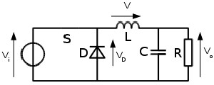
When the switch is closed, current from input flows through the inductor, the inductor doesn’t allow sudden changes in the current, hence the current across inductor is converted into magnetic field, thus the inductor starts to charge up. Therefore, when the switch is closed, the capacitor also stores the charge.
Stage 2: When the switch is open
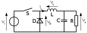
Now the switch is OFF and no current is passing through the inductor, and the inductor is acting as a supply and the capacitor also acts in smoothing out the output when inductor loses the energy. The process is repeated when the switch is closed again.
We can get any output voltage between 0 and input voltage by changing the duty cycle.
Buck Converter using 555 Timer
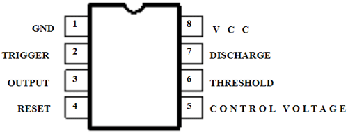
In order to make the system work in real world application, we need to switch on and off the switch a lot faster than a human can perform. Therefore, we use a PWM pulse generator and a transistor as a switch to perform the task. A 555 timer IC in Astable mode can be used to generate the PWM output for our operation. The IC 555 generates around 30 KHz frequency with the help of passive and active components connected to it. The pinout diagram of NE555 is given below.
Formula to Calculate PWM Frequency and Duty cycle on 555 Timer
For designing the circuit, we used the IC 555 timer in Astable mode. Here, the output pulse is continuously switched between high and low states. To change the frequency of the oscillation, we can change the values of Resistor and capacitor (RC) network, connected with the 555 timer. The above values for our circuit was selected using the formula written below:
ON time (sec) = 0.693 * (R1 + R2) * C
OFF time (sec) = 0.693 * R2 * C
Frequency = 1.44 / ((R1 + R2 + R2) * C)
Duty cycle D = PW/T,
Here,
D is the duty cycle, PW is the pulse width (pulse active time), and T is the total period of the signal, all the values of resistors are in Ohm and values of capacitors are in Farads.
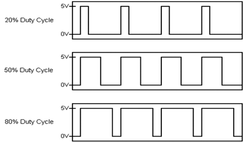
The above image shows the waveform in different duty cycle. We can easily say that the higher duty cycle means that the device is energized for longer durations.
555 Timer based Buck Regulator Circuit Diagram
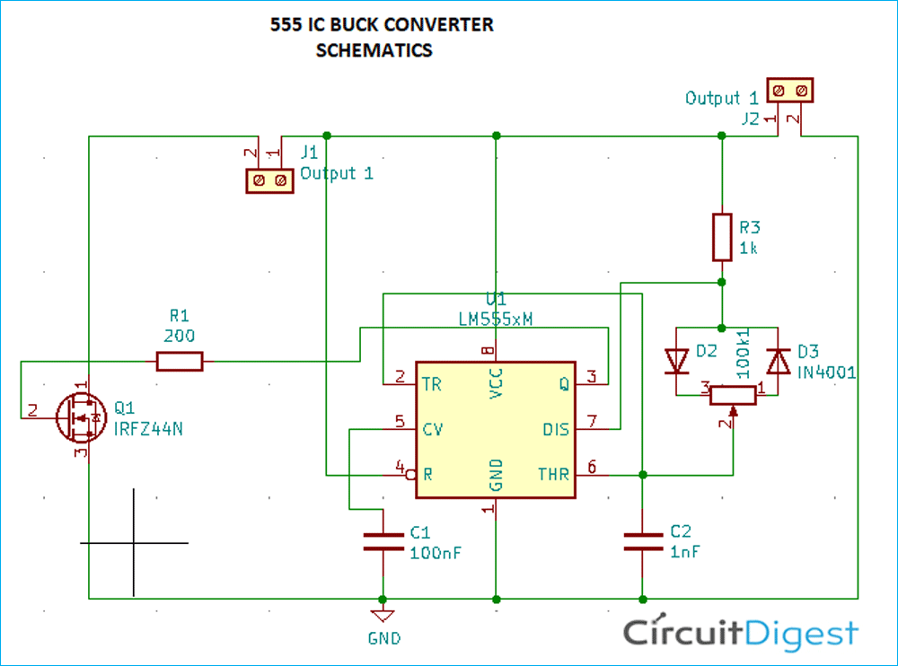
I designed a rough circuit in paper and calculated the components based on the above formulae and selected the components based on the outcome. The Buck Regulator circuit using 555 Timer is shown below:
Components required for our project:
- 1 x NE555
- 1 x IRFZ44N – N Channel mosfet
- 1 x 200 R, Resistor
- 1 x 1K, Resistor
- 3 x IN4001 Diode
- 1 x 100nF, Capacitor
- 1 x 1nF Capacitor
- 1 x 100k potentiometer
- 2 x 2pin connector
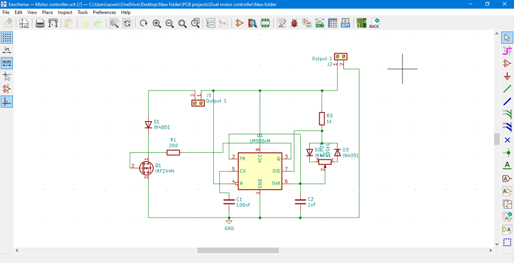
The circuit uses the 555 IC as the PWM generator and hence the whole circuit is based around the same. The connections of all 8 pins are mentioned below.
- Pin 1 is connected to the ground rail.
- Pin 2 and pin 6, with the ground through a 1nF capacitor.
- Pin 3 is connected to the gate of the mosfet. This pin sends the pwm output to the gate of the MOSFET.
- Pin 4 is connected to the +ve input rail.
- Pin 5 is connected to the ground with a 100nF capacitor. It helps in stabilizing the output and provide immunity against electrical noises.
- Pin 7 is connected to the +ve input with a 1k resistor and is also connected to the inverted diode setup.
- Pin 8 is connected to the +ve rail.
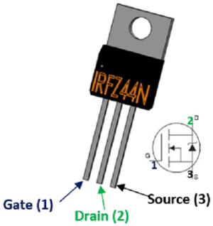
In the circuit above, the N-channel MOSFET, IRFZ44N is used as a switch, driven by the faint signal from IC 555. The Drain of this Mosfet is providing the negative switching control to the circuit. It has the following specifications.
- VDSS = 55V
- RDS(on) = 17.5mΩ
- ID = 49A
Building and Testing our Buck Regulator circuit
I used KiCad to design the schematics. The image attached below shows the screenshot of the KiCad screen. After designing the schematics, we assigned the proper footprints for all the components and arranged the components in the PCB editor tool. After laying out all the components in a satisfactory manner, the next step was to take a printout of the design in order to etch the PCB.
The image given below shows the steps by step illustration of how the PCB was manufactured and tested. You can also check out the article on how to make home-made PCBs if you are interested in making this PCB on your own. The gerber file used in this project can be downloaded from below.
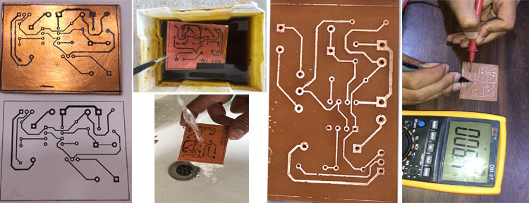
The Print was transferred to copper clad plate using a hot iron, which left the impression of the circuit on the plate, which was obtained by removing the paper from the copper clad by dissolving it in water. The impression was left on the plate. We then dipped the board in the Ferrous Chloride solution (PCB etching powder), which removed the excess copper and only the tracks were left on the board. We tested the continuity of the track using the multimeter and when got satisfied, using a PCB hand drill, all the holes were made in the required position.
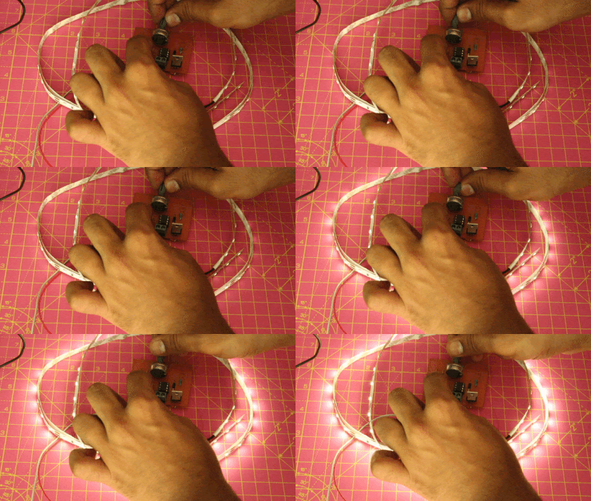
We soldered all the components in place and used a 12V LED strip to see the product in action. For the input, I used a voltage supply, supplying a constant 11V output. By rotating the potentiometer, the LED strip’s brightness could be adjusted.
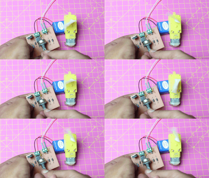
A 12 V DC motor was also tested with the setup. The working remains the same, i.e. the duty cycle is changed by adjusting the input resistances therefore by rotating the potentiometer, the speed of a DC motor was changed as shown in the GIF below.
Now, where can you use a Buck regulator like this?
Buck converters are used in a lot of applications where efficiency is paramount, some applications includes, battery chargers, power amplifiers, quad copters, powertrain and battery chargers of EVs, Medical application, smart phones, laptops and are also used in motor controllers, etc.
Conclusion
A 555 IC based converter is one of the simplest, yet efficient method to keep the complexity as well as the cost of your project low while achieving a high efficiency and improving lifespan of your components. This easy power electronics circuit can step down a DC voltage with efficiency as high as 95% compared to 40-60% efficiency of a linear voltage regulators. This driving technique is also useful for the speed control of a motor and dimming LEDs without effecting it’s lifespan, making it a very versatile voltage control option for electronics project.
If you have any questions or doubt regarding this article, please feel free to use our Forum or you can leave your comments below.

