Registers are common electronic components that are used in devices to store data. These are the smallest data holding elements which store the operands or instructions that are being processed by the CPU. There are different types of Registers, namely Instruction Registers, Program Registers, ALU Registers, General Purpose Registers, and so on. They differ in the number of bits that can be stored depending upon the configuration of the system.
In this tutorial, we are going to learn how to implement a simple Register in VHDL. If you are new to VHDL, refer to our previous VHDL tutorials using ModelSim.
Before learning how to implement in VHDL, we shall see the available ports in a Register.
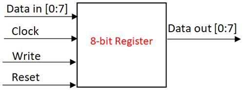
Registers: Registers are sequential memory storing devices. Here, the term sequential refers to “it’s a clocked circuit” which means it is controlled by a clock. These Registers vary in size from one system to the other (some maybe 8 bit, some maybe 4 bit). Other than that, the Register has a data in and data out port. A reset pin to erase the contents of the Registers and a write signal to write the data into the Register are also available. So, a typical register will have a clock, write, reset, data in, and data out port. The schematic diagram for an 8-bit register is given below.

Since it’s a clocked circuit, the data will get loaded only when the clock is active (clock=”1”) and the Write signal is active (write=”1”). When the reset signal is high (reset=”1”), the data stored will be erased, it will get assigned to “00000000”.
The events that take place concerning clock, write and reset are given below.
|
Clock |
Write |
Reset |
Data out |
|
1 |
1 |
-- |
Data loaded |
|
0 |
1 |
-- |
No data loaded |
|
1 |
0 |
-- |
No data loaded |
|
0 |
0 |
-- |
No data loaded |
|
1 |
0 |
1 |
Data Reset |
|
0 |
0 |
1 |
No Data Reset |
Now that we know the basics of the registers, we shall see how to implement them in VHDL.
How to implement Registers in VHDL?
First, I will give the full code for the registers, which we will break down into smaller snippets for better understanding.
VHDL Code for Registers
Library IEEE;
use IEEE.std_logic_1164.all;
entity reg_a is
port ( signalrega_input :in  std_logic_vector(7 downto 0) ;
signal writ: in std_logic;
signal reset: in std_logic;
signal clk: in std_logic;
signal rega_output: out std_logic_vector(7 downto 0)
 );
end reg_a;
architecture sim of reg_a is
 begin
process(clk) is
   begin
 if rising_edge(clk) then
if(writ='1') then
rega_output<=rega_input;
elsif(reset='1') then
rega_output<="00000000";
end if;
      end if;
        end process;
end sim;
At first, the Libraries are imported, the entity is declared with the label “reg_a” and data in, data out, clock, write, reset signal is declared.
Library IEEE;
use IEEE.std_logic_1164.all;
entity reg_a is
port ( signalrega_input :in  std_logic_vector(7 downto 0) ;
signal writ: in std_logic;
signal reset: in std_logic;
signal clk: in std_logic;
signal rega_output: out std_logic_vector(7 downto 0)
 );
end reg_a;
After that, we have declared the architecture with the label “sim” associated with the entity label “reg_a”.
Process(clk): Since the whole circuit depends on the clock's function, we have to process the clock.
if rising_edge(clk) then: “rising_edge(clk)” means the point where the clock’s signal is “1”. So, only if the clock's signal is “1” it passes on to the next ‘if’ condition.
The ‘if’ conditions concerning write and reset are given. So, if the write signal is “1” the data will be loaded. If the reset signal is “1” the data will be reset to “0000000”.
Note: While reset=1, always remember to set write=0, only then the data will be reset.
architecture sim of reg_a is
 begin
process(clk) is
   begin
 if rising_edge(clk) then
if(writ='1') then
rega_output<=rega_input;
elsif(reset='1') then
rega_output<="00000000";
end if;
      end if;
        end process;
end sim;
Just copy-paste this code in the ModelSim, compile, and simulate the same. For compilation and simulation process, refer to “implementation of basic logic gates using ModelSim”.
I have just compiled and simulated the code, and the following waveforms are obtained.
|
Timing(ps) |
Data in |
Clock |
Write |
Reset |
Data out |
|
0-100 |
11111111 |
1,0 |
---- |
--- |
----- |
|
100-200 |
11111111 |
1,0 |
--- |
--- |
--- |
|
200-300 |
11111111 |
1,0 |
1 |
--- |
11111111 |
|
300-400 |
10101010 |
1,0 |
1 |
---- |
11111111 |
|
400-500 |
10101010 |
1,0 |
1 |
---- |
10101010 |
|
500-600 |
10101010 |
1,0 |
0 |
1 |
10101010 |
|
600-700 |
10101010 |
1,0 |
0 |
1 |
00000000 |
|
700-800 |
11110000 |
1,0 |
1 |
0 |
00000000 |
|
800-900 |
11110000 |
1,0 |
1 |
0 |
11110000 |
|
|
|
|
|
|
|
Just move the cursor along the waveform, we can see that the data gets stored only if both clock and write signal is 1. ‘U’ represents undefined. Also, since it’s a sequential circuit, there will be some minimal delay for updating the contents, but it will get updated in the next positive clock cycle.
Library IEEE;
use IEEE.std_logic_1164.all;
entity reg_a is
port ( signal rega_input :in std_logic_vector(7 downto 0) ;
signal writ: in std_logic;
signal reset: in std_logic;
signal clk: in std_logic;
signal rega_output: out std_logic_vector(7 downto 0)
);
end reg_a;
architecture sim of reg_a is
begin
process(clk) is
begin
if rising_edge(clk) then
if(writ='1') then
rega_output<=rega_input;
elsif(reset='1') then
rega_output<="00000000";
end if;
end if;
end process;
end sim;


