All microcontrollers have specific numbers of IO pins but in some applications, like in a 7-Segment Display, we will need more GPIO pins than what our controller could offer. For such cases, where multiple output pins are required but the microcontroller has a limited number of output pins, 74HC595 Shift Register would be a perfect choice. 74HC595 is a shift register that takes serial data as an input and provides parallel output. Other than the power pins, it requires only 3 pins that need to control multiple shift registers. We have previously this IC with other microcontrollers as well
Therefore, one can use three output pins from the microcontroller unit and cascade two or more shift registers to get 16 or 24+ output pins. In this ESP32 74HC595 project, we will interface three 74HC595 using only three pins and connect three 7-Segment displays to see outputs using only three pins from the ESP32 which is a WiFi/BT enabled microcontroller device that is a popular choice for many IoT based projects. You can also check out other ESP32 Projects if you are interested in building more with this controller. Also, we will be using the Arduino IDE to program our ESP32 here, if you completely new, do check out the Getting started with ESP32 using Arduino before you proceed any further.
Required Components
- ESP32 Devkit v4.0
- 7-Seg displays common cathode - 3pcs
- 74HC595 - 3 pcs
- 680R resistor - 24pcs
- 5V power supply
- Breadboard
- Lots of hook up wires
- Arduino IDE with ESP32 programming environment.
- A micro-USB cable
Schematic
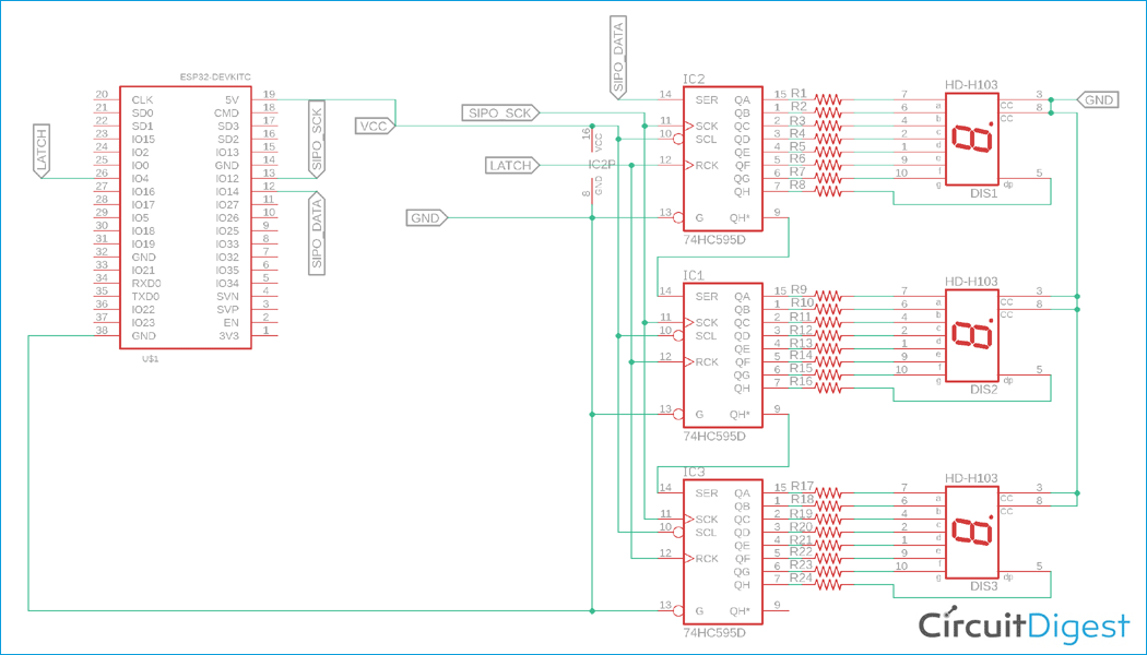
The schematic diagram for ESP32 7 Segment Display is given below-
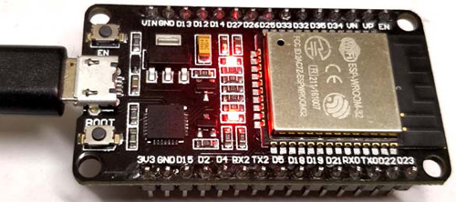
The ESP32 is connected with the 74HC595. The data pin of the shift register is connected with the PIN14, the Clock pin is connected with the PIN12, and the Latch or strobe pin is connected with the PIN4. You can check out the basics of 7-Segment Display article to understand more about 7-segment displays and how they work.
74HC595 Shift Register
74HC595 is an 8-bit shift register. The pin diagram can be shown in the below image-

The pin description can be seen in the below table-
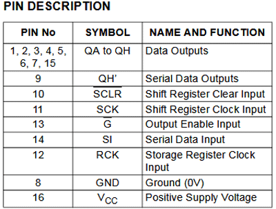
The QA to QH, from the starting pin 1 to 7 and the pin 15 is the 8-bit output from the shift register. The input pin is PIN14 that is serial data input that takes the data serially.
Other input pins are PIN 11 and PIN12. Those two pins are SCK and RCK. SCK is the clock input and the RCK is the latch input. The truth table that is required to get the data and provide the data to the next shift register is given below
74HC595 Truth Table
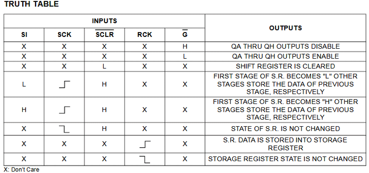
However, PIN9 is the serial data output which will provide the data to the next cascaded shift register. Thus, PIN9 is connected with the PIN 14 of the next shift register. The data gets passed serially to the next shift register continuously.
Programming ESP32 for 7 Segment Display using 74HC595
The program to control all three 7-Segment Display can be found at the bottom of the page. You can directly use it for the above given circuit diagram and test it. The explanation of the code is as follows.
Before we get into the program, we declare the type of 7-Segment Display we are using.
This line will identify the ESP32 about the 7-Segment display type. If the common cathode is used, it needs to be true, otherwise, if the common anode is used, it requires to be false. Since depending on the common Cathode status, the output of the shift register will change.
const bool commonCathode = true;
The next section is used to provide the supported digit and letters in an 8-bit format. This will provide the exact binary output from the shift register to light up the 7-Seg displays.
const byte digit_pattern[17] =
{
  // 74HC595 Outpin Connection with 7segment display.
  // Q0 Q1 Q2 Q3 Q4 Q5 Q6 Q7
  // a  b  c  d  e  f  g  DP
  0b11111100,  // 0
  0b01100000,  // 1
  0b11011010,  // 2
  0b11110010,  // 3
  0b01100110,  // 4
  0b10110110,  // 5
  0b10111110,  // 6
  0b11100000,  // 7
  0b11111110,  // 8
  0b11110110,  // 9
  0b11101110,  // A
  0b00111110,  // b
  0b00011010,  // C
  0b01111010,  // d
  0b10011110,  // E
  0b10001110,  // F
  0b00000001   // .
};
In the below code lines, the shift register pins are defined.
//Pin connected to ST_CP of 74HC595
int latchPin = 4;
//Pin connected to SH_CP of 74HC595
int clkPin = 12;
//Pin connected to DS of 74HC595
int dtPin = 14;
// display value
int dispVal = 0;
bool increment = true;
The setup code is done before the actual loop application. In the above code, the 74HC595 control pins are set as output and the serial output for UART communication is also done for the debugging purpose only.
void setup() {
  // put your setup code here, to run once:
  // set the serial port at 115200
  Serial.begin(115200);
  delay(1000);
  // set the 74HC595 Control pin as output
  pinMode(latchPin, OUTPUT);    //ST_CP of 74HC595
  pinMode(clkPin, OUTPUT);      //SH_CP of 74HC595
  pinMode(dtPin, OUTPUT);       //DS of 74HC595
}
In the loop section or the actual application section, the code has two-part. At first, the digits are incremented and on the other part, the digits are decremented. However, writing into the shift register is always begging with the latch pin becoming LOW, and after the data is sent, it needs to be High.
void loop() {
  // put your main code here, to run repeatedly:
  int dispDigit1=dispVal/10;
  int dispDigit2=dispVal%10;
  if(increment==true){
    printf("%d%d.\n", dispDigit1,dispDigit2);
    digitalWrite(latchPin, LOW);
    if(commonCathode == true){
      shiftOut(dtPin, clkPin, LSBFIRST, digit_pattern[dispDigit2]|digit_pattern[16]);   // 1. (Digit+DP)
      shiftOut(dtPin, clkPin, LSBFIRST, digit_pattern[dispDigit1]);
    }else{
      shiftOut(dtPin, clkPin, LSBFIRST, ~(digit_pattern[dispDigit2]|digit_pattern[16]));   // 1. (Digit+DP)
      shiftOut(dtPin, clkPin, LSBFIRST, ~(digit_pattern[dispDigit1]));
    }
    digitalWrite(latchPin, HIGH);
    dispVal += 1;
    if (dispVal == 99){
      increment=false;
    }
  }else{
    printf("%d%d.\n", dispDigit1,dispDigit2);
    digitalWrite(latchPin, LOW);
    if(commonCathode == true){
      shiftOut(dtPin, clkPin, LSBFIRST, digit_pattern[dispDigit2]|digit_pattern[16]);   // 1. (Digit+DP)
      shiftOut(dtPin, clkPin, LSBFIRST, digit_pattern[dispDigit1]);
    }else{
      shiftOut(dtPin, clkPin, LSBFIRST, ~(digit_pattern[dispDigit2]|digit_pattern[16]));   // 1. (Digit+DP)
      shiftOut(dtPin, clkPin, LSBFIRST, ~(digit_pattern[dispDigit1]));
    }
    digitalWrite(latchPin, HIGH);
    dispVal -= 1;
    if (dispVal == 0){
      increment=true;
    }
  }
  delay(250);
}
digitalWrite(latchPin, LOW);
The data that is sent in between this Low and High code.
digitalWrite(latchPin, HIGH);
Then, if the common cathode is used, it will print the digit in the 7-Seg display by using the below code -
shiftOut(dtPin, clkPin, LSBFIRST, digit_pattern[dispDigit2]|digit_pattern[16]);
shiftOut(dtPin, clkPin, LSBFIRST, digit_pattern[dispDigit1]);
These shift Out function uses the bitwise operator to shift the data serially along with the clock input at the same time. It will print the digit as well as the data point (DP). However, since it is an LSB First data, the LSB is first sent to the 74HC595 and shifted to the next 74HC595. The third 7-Segment is not programmed and connected to see that the first digit is transferred to the last 7-segment, i.e. 74HC595 unit. When the 7-Seg is a common anode, it will use an invert operator to invert the output. Thus,
shiftOut(dtPin, clkPin, LSBFIRST, ~(digit_pattern[dispDigit2]|digit_pattern[16]));
shiftOut(dtPin, clkPin, LSBFIRST, ~(digit_pattern[dispDigit1]));
Seven Segment Display with ESP32 – Working
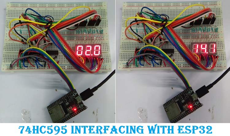
The circuit is constructed in two breadboards and the output is checked. The digits are shown perfectly on the 7-Seg displays as you can see in the below image. The connections and debugging might get hard because of the number of wires, we build it on a breadboard and it did work as expected.
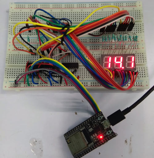
The complete working can be found in the video linked at the bottom of this page. Hope you enjoyed the tutorial and learned something useful, if you have any questions, leave them in the comment section or use our forums for other technical questions and discussions.
/*
 * This program Print Numbers on 3, 7segment display
 * Hardware Connections (Breakoutboard to Arduino Nano):
 * Vin  - 5V (3.3V is allowed)
 * GND - GNDs
 * 74HC595 ST_CP - 4 (ESP32)
 * 74HC595 SH_CP - 12 (ESP32)
 * 74HC595 DS - 14 (ESP32)
 *
 */
// set the 7segment type (common Cathode or Anode)
const bool commonCathode = true; // I'm using common Cathode 7segment if you use common Anode then change the value into false.
// alpha-digit pattern for a 7-segment display
const byte digit_pattern[17] =
{
  // 74HC595 Outpin Connection with 7segment display.
  // Q0 Q1 Q2 Q3 Q4 Q5 Q6 Q7
  // a  b  c  d  e  f  g  DP
  0b11111100,  // 0
  0b01100000,  // 1
  0b11011010,  // 2
  0b11110010,  // 3
  0b01100110,  // 4
  0b10110110,  // 5
  0b10111110,  // 6
  0b11100000,  // 7
  0b11111110,  // 8
  0b11110110,  // 9
  0b11101110,  // A
  0b00111110,  // b
  0b00011010,  // C
  0b01111010,  // d
  0b10011110,  // E
  0b10001110,  // F
  0b00000001   // .
};
//Pin connected to ST_CP of 74HC595
int latchPin = 4;
//Pin connected to SH_CP of 74HC595
int clkPin = 12;
//Pin connected to DS of 74HC595
int dtPin = 14;
// display value
int dispVal = 0;
bool increment = true;
void setup() {
  // put your setup code here, to run once:
  // set the serial port at 115200
  Serial.begin(115200);
  delay(1000);
  // set the 74HC595 Control pin as output
  pinMode(latchPin, OUTPUT);    //ST_CP of 74HC595
  pinMode(clkPin, OUTPUT);      //SH_CP of 74HC595
  pinMode(dtPin, OUTPUT);       //DS of 74HC595
}
void loop() {
  // put your main code here, to run repeatedly:
  int dispDigit1=dispVal/10;
  int dispDigit2=dispVal%10;
  if(increment==true){
    printf("%d%d.\n", dispDigit1,dispDigit2);
    digitalWrite(latchPin, LOW);
    if(commonCathode == true){
      shiftOut(dtPin, clkPin, LSBFIRST, digit_pattern[dispDigit2]|digit_pattern[16]);   // 1. (Digit+DP)
      shiftOut(dtPin, clkPin, LSBFIRST, digit_pattern[dispDigit1]);
    }else{
      shiftOut(dtPin, clkPin, LSBFIRST, ~(digit_pattern[dispDigit2]|digit_pattern[16]));   // 1. (Digit+DP)
      shiftOut(dtPin, clkPin, LSBFIRST, ~(digit_pattern[dispDigit1]));
    }
    digitalWrite(latchPin, HIGH);
    dispVal += 1;
    if (dispVal == 99){
      increment=false;
    }
  }else{
    printf("%d%d.\n", dispDigit1,dispDigit2);
    digitalWrite(latchPin, LOW);
    if(commonCathode == true){
      shiftOut(dtPin, clkPin, LSBFIRST, digit_pattern[dispDigit2]|digit_pattern[16]);   // 1. (Digit+DP)
      shiftOut(dtPin, clkPin, LSBFIRST, digit_pattern[dispDigit1]);
    }else{
      shiftOut(dtPin, clkPin, LSBFIRST, ~(digit_pattern[dispDigit2]|digit_pattern[16]));   // 1. (Digit+DP)
      shiftOut(dtPin, clkPin, LSBFIRST, ~(digit_pattern[dispDigit1]));
    }
    digitalWrite(latchPin, HIGH);
    dispVal -= 1;
    if (dispVal == 0){
      increment=true;
    }
  }
  delay(250);
}
