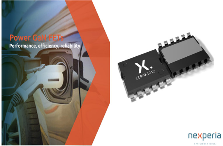
Nexperia has introduced a new range of GaN FET devices that consists of next-gen high-voltage Gan HEMT H2 technology in both TO-247 and CCPAK surface-mount packaging. The GaN technology employs through-epi vias for reducing defects and shrinking the die size up to 24%. The TO-247 package reduces the RDS (on) by 41mΩ (max., 35 mΩ types. at 25 °C) with high threshold voltage and low diode forward voltage. Whereas the CCPAK surface mount package will further reduce the RDS (on) to 39 mΩ (max., 33 mΩ typ. at 25 °C).
The device can be driven simply using standard Si MOSFET as the part is configured as cascade devices. The CCPAK surface-mount packaging adopts Nexperia’s innovative copper-clip package technology to replace internal bond wires, this also reduces the parasitic losses optimizes electrical and thermal performance and improves reliability. The CCPAK GaN FETs are available in top-or bottom cooled configuration for improved heat dissipation.
Both versions meet the demands of AEC-Q101 for automotive applications and other applications include on-board chargers, DC/DC converters and traction inverters in electric vehicles, and industrial power supplies in the 1.5-5 kW range for titanium-grade rack-mounted telecoms, 5G, and datacenters.

