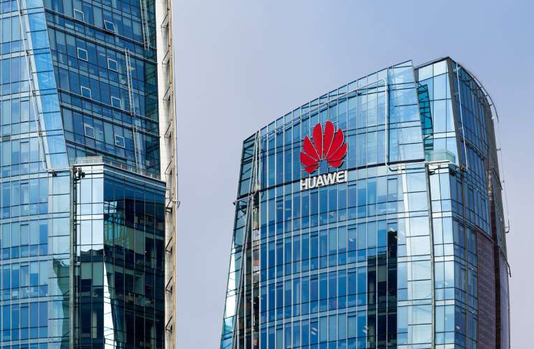
The Semiconductor Industry Association (SIA) has stated that Huawei has already acquired two semiconductor units and is now planning to set-up another three
A Bloomberg undercover reporting has now revealed that China’s largest global technology firm Huawei is setting-up a wide range semiconductor fabs throughout the country to evade US sanctions. A year back, Huawei had already proclaimed to enter intro chipset manufacturing for which it has received state from the government worth $30 billion.
The Semiconductor Industry Association (SIA) has stated that Huawei has already acquired two semiconductor units and is now planning to set-up another three. Moreover, the US Commerce department also added that Huawei is currently in the export control list from 2019 as ordered by the Trump government keeping in mind internal security concerns.
Now, the point is if as per SIA report Huawei is setting-up fab units under the umbrella of other firms, then it could outwit US export restrictions order and successfully buy US-based chipmaking equipment. When news agency Reuters approached both SIA and Huawei for further clarifications, they did not respond to any queries.
As per the export restriction law unleashed by the then President Donald Trump, Huawei has been caged on a trade embargo and most of the suppliers in the country were even barred from providing advanced technology and shipping products to the firm unless they acquire proper licenses. Officials made the restrictions more strict in an effort to weaken Huawei’s ability to manufacture and design semiconductor chips.
Back in march 2023, Huawei had stated that they are now equipped with their own semiconductor design tools so that it becomes self-reliant in the semiconductor industry. Eric Xu of Huawei told the media that in association with other Chinese companies they have built the electronic electronic chip design tools that are needed to manufacture chips at 14-nm and above.
Pranay Kotasthane, chairperson of the high tech geopolitics program at the Takshashila Institution, told CNB, "I would wait to see more details before knowing how effective Huawei’s design tools are. Kotasthane explained that contract chip manufacturing firms, also known as foundries, work with semiconductor design companies to come up with a set of files called a Process Design Kit. This PDK “models the physical and electrical characteristics” of the basic components of a chip."
"The design firm and manufacturer needs to go through a process to optimize the production to ensure the highest yield of semiconductors. If this process does not happen, then “chip designs will fail when converted into silicon. There’s not enough proof yet to suggest that Chinese EDA [electronic design automation] companies have crossed this barrier," added Kotasthane.

