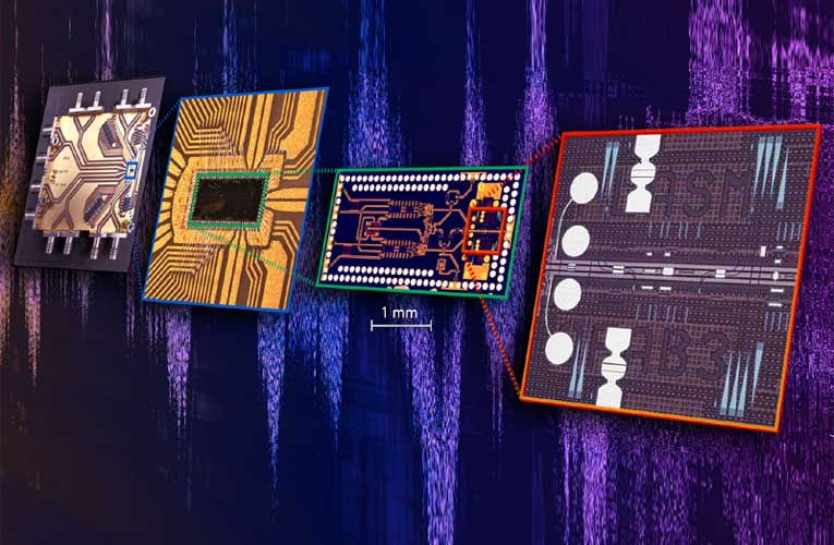
Researchers from ETH Zurich have come up with an ultrafast chip to be used for converting fast electronic signals directly into ultrafast light signals with no loss of signal quality. This is the first time ever that the electronic and light-based elements have been combined on the same chip. The experiment was performed in collaboration with partners in Germany, US, Israel, and Greece. This is the stepping stone in technical terms as currently, these elements have to be manufactured on separate chips and then connected up with wires.
When electronic signals are converted into light signals using separate chips, the amount of signal quality lessens down and the speed of data transmission using light too gets hampered. However, this is not the case with the new plasmonic chip that comes with a modulator, a component on the chip that generates light of a given intensity by converting the electrical signals into light waves. The small size of the modulator ensures there is no loss of quality and intensity in the conversion process, and light, rather the data is transmitted speedily. The combination of electronics and plasmonics on a single chip makes amplification of light signals possible and ensures faster data transmission.
The electronic and photonic components are placed tightly on top of one another, like two layers, and are directly placed on the chip using “on-chip vias” to make it as compact as possible. This layering of the electronics and photonics shortens transmission paths and reduces losses in terms of signal quality. This approach is aptly called “monolithic co-integration” as the electronics and photonics are implemented on one single substrate. The photonic layer on the chip contains a plasmonic intensity modulator that helps in converting electrical signals into even faster optical ones because of the metal structures that channel the light to reach higher speeds.
The four lower-speed input signals are bundled and amplified to form a high-speed electrical signal which is then converted into a high-speed optical signal. This process is known as “4:1 multiplexing” which for the first time has made the transmission of data on a monolithic chip at a speed of over 100 gigabits per second possible. The high speed was achieved by combining plasmonics with classical CMOS electronics and even faster BiCMOS technology. Besides, new temperature-stable, electro-optical material from the University of Washington and insights from the Horizon 2020 projects PLASMOfab and plaCMOS were also used. The researchers are convinced that this ultrafast chip will fast pave the way for speedy data transmission in optical communication networks of the future.

