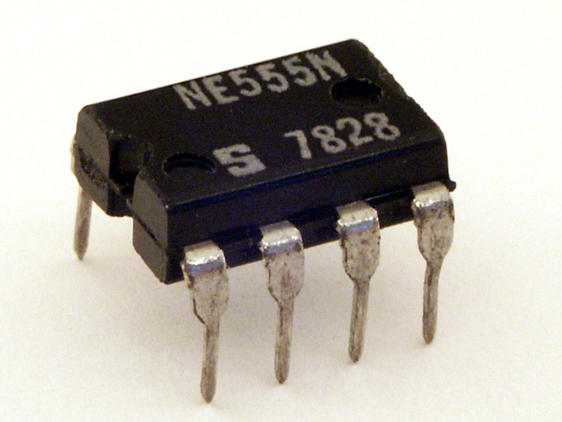
555 Timer IC is one of the commonly used IC among students and hobbyists. There are a lot of applications of this IC, mostly used as vibrators like, ASTABLE MULTIVIBRATOR, MONOSTABLE MULTIVIBRATOR, and BISTABLE MULTIVIBRATOR. You can find here some circuits based on 5555 IC. This tutorial covers different aspects of 555 Timer IC and explains its working in details. So lets first understand what are astable, monostable and bistable vibrators.
ASTABLE MULTIVIBRATOR
This means there will be no stable level at the output. So the output will be swinging between high and low. This character of unstable output is used as clock or square wave output for many applications.
[Understand more about astable multivibrator: 555 Timer Astable Multivibrator Circuit]
MONOSTABLE MULTIVIBRATOR
This means there will be one stable state and one unstable state. The stable state can be chosen either high or low by the user. If the stable output is selected high, then the timer always tries to put high at output. So when a interrupt is given, the timer goes low for a short time and since the low state is unstable it goes to high after that time. If the stable state is chosen low, with interrupt the output goes high for a short time before coming to low.
[Understand more about monostable multivibrator: 555 Timer Monostable Multivibrator Circuit]
BISTABLE MULTIVIBRATOR
This means both the output states are stable. With each interruption the output changes and stays there. For instance the output is considered high now with interruption it goes low and it stays low. By the next interruption it goes high.
[Understand more about bistable multivibrator: 555 Timer IC Bistable Multivibrator Circuit]
Important Characterstics of 555 Timer IC
NE555 IC is a 8 pin device. The important electrical characteristics of timer are that it should not be operated above 15V, it means the source voltage cannot be higher than 15v. Second, we cannot draw more than 100mA from the chip. If don't follow these, IC would be burnt and damaged.
Working Explanation
The timer basically consists of two primary building blocks and they are:
1.Comparators (two) or two op-amp
2.One SR flip-flop (set reset flip-flop)
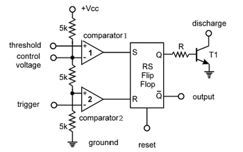
As shown in the above figure there are only two important components in timer, they are comparator and flip-flop. Lets understand what are comparators and flip flops.
Comparators: comparator is simply a device that compares the voltages at the input terminals (inverting (- VE) and non-inverting (+VE) terminals). So depending on the difference in the positive terminal and negative terminal at input port, the output of the comparator is determined.
For example consider positive input terminal voltage be +5V and negative input terminal voltage be +3V. The difference is, 5-3=+2v. Since the difference is positive we get the positive peak voltage at the output of the comparator.
For another example, if positive terminal voltage is +3V and negative input terminal voltage be +5V. The difference is +3-+5=-2V, since the difference input voltage is negative. The output of comparator will be negative peak voltage.
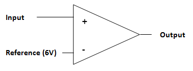
If for an example consider the positive input terminal as INPUT and the negative input terminal as REFERENCE as shown in above figure. So the difference of voltage between INPUT and REFERNCE is positive we get a positive output from the comparator. If the difference is negative then we will get negative or ground at the comparator output.
Flip-Flop: The flip-flop is a memory cell, it can store one bit of data. In the figure we can see the truth table of SR flip-flop.
There are four states to a flip-flop for two inputs; however we need to understand only two states of the flip- flop for this case.
| S | R | Q | Q' (Q bar) |
| 0 | 1 | 0 | 1 |
| 1 | 0 | 1 | 0 |
Now as show in the table, for set and reset inputs we get the respective outputs. If there is a pulse at the set pin and a low level at reset, then flip-flop stores the value one and puts high logic at Q terminal. This state continues until the reset pin gets a pulse while set pin has low logic. This resets the flip-flop so the output Q goes low and this state continues until the flip-flop is set again.
By this way the flip-flop stores one bit of data. Here another thing is Q and Q bar are always opposite.
In a timer the comparator and flip-flop are brought together.
Consider 9V is supplied to the timer, because of the voltage divider formed by the resistor network inside the timer as shown in the block diagram; there will be voltage at the comparator pins. So because of the voltage divider network we will have +6V at the negative terminal of the comparator one. And +3V at the positive terminal of the second comparator.
One another thing is comparator one output is connected to reset pin of flip-flop, so it the comparator one output goes high from low then the flip-flop will reset. And on the other hand the second comparator output is connected to set pin of flip-flop, so if the second comparator output goes high from low the flip-flop sets and stores ONE.
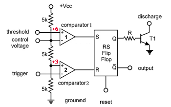
Now if we observe carefully, for a voltage less than +3V at the trigger pin (negative input of second comparator), the output of the comparator goes low from high as discussed earlier. This pulse sets the flip-flop and it stores a value one.
Now if we apply a voltage higher than +6V at the threshold pin (positive input of comparator one) , the output of comparator goes from low to high. This pulse resets the flip-flop and the flip-flip store zero.
Another thing happens during reset of flip-flop, when it resets the discharge pin gets connected to ground as Q1 gets turned on. Q1 transistor turns on because the Qbar is high at reset and is connected to Q1 base.
In astable configuration the capacitor connected here discharges during this time and so the output of timer will be low during this time.In astable configuration the time during the capacitor charges the trigger pin voltage will be less than +3V and so the flip-flop will store one and the output will be high.
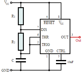
In an astable configuration as shown in figure,
The output signal frequency depends on RA, RB resistors and capacitor C. The equation is given as,
Frequency(F) = 1/(Time period) = 1.44/((RA+RB*2)*C).
Here RA, RB are resistance values and C is capacitance value. By putting the resistance and capacitance values in above equation we get the frequency of output square wave.
High Level logic time is given as, TH= 0.693*(RA+RB)*C
Low Level logic time is given as, TL= 0.693*RB*C
Duty ratio of the output square wave is given as, Duty Cycle= (RA+RB)/(RA+2*RB).
555 Timer Pin Diagram and Descriptions
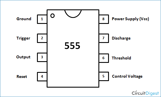
Now as shown in figure, there are eight pins for a 555 Timer IC namely,
1.Ground.
2.Trigger.
3.Output.
4.Reset.
5.Control
6.Threshold.
7.Discharge
8.Power or Vcc
Pin 1. Ground: This pin has no special function what so ever. It is connected to ground as usual. For the timer to function, this pin must and should be connected to ground.
Pin 8. Power or VCC: This pin also has no special function. It is connected to positive voltage. For the timer to function to work, this pin must be connected to positive voltage of range +3.6v to +15v.
Pin 4. Reset: As discussed earlier, there is a flip-flop in the timer chip. The output of flip-flop controls the chip output at pin3 directly.
Reset pin is directly connected to MR (Master Reset) of the flip-flop. On observation we can observe a small circle at the MR of flip-flop. This bubble represents the MR (Master Reset) pin is active LOW trigger. That means for the flip-flop to reset the MR pin voltage must go from HIGH to LOW. With this step down logic the flip-flop gets hardly pulled down to LOW. So the output goes LOW, irrespective of any pins.
This pin is connected to VCC for the flip-flop to stop from hard resetting.
Pin 3. OUTPUT: This pin also has no special function. This pin is drawn from PUSH-PULL configuration formed by transistors.
The push pull configuration is shown in figure. The bases of two transistors are connected to flip-flop output. So when logic high appears at the output of flip-flop, the NPN transistor turns on and +V1 appears at the output. When logic appeared at the output of flip-flop is LOW, the PNP transistor gets turned on and the output pulled down to ground or –V1 appears at the output.
Thus how the push-pull configuration is used to get square wave at the output by control logic from flip-flop. The main purpose of this configuration is to get the load off flip-flop back. Well the flip-flop obviously cannot deliver 100mA at the output.
Well until now we discussed pins that do not alter the condition of output at any condition. The remaining four pins are special because they determine the output state of timer chip, we will discuss each of them now.
Pin 5. Conrol Pin: The control pin is connected from the negative input pin of comparator one.
Consider for a case the voltage between VCC and GROUND is 9v. Because of the voltage divider in the chip as observed in figure3 of page8, The voltage at the control pin will be VCC*2/3 (for VCC = 9, pin voltage=9*2/3=6V ).
The function of this pin to give the user the directly control over first comparator. As shown in above figure the output of comparator one is fed to the reset of flip-flop. At this pin we can put a different voltage, say if we connect it to +8v. Now what happens is, the THRESHOLD pin voltage must reach +8V to reset the flip-flop and to drag the output down.
For normal case, the V-out will go low once the capacitor gets charge up to 2/3VCC (+6V for 9V supply). Now since we put up a different voltage at control pin (comparator one negative or reset comparator).
Capacitor should charge until its voltage reaches the control pin voltage. Because of this force capacitor charging, the turn on time and turn off time of signal changes. So the output experiences a different turn on torn off ration.
Normally this pin is pulled down with a capacitor. To avoid unwanted noise interference with the working.
Pin 2. TRIGGER: Trigger pin is dragged from the negative input of comparator two. The comparator two output is connected to SET pin of flip-flop. With the comparator two output high we get high voltage at the timer output. So we can say the trigger pin controls timer output.
Now here what to observe is, low voltage at the trigger pin forces the output voltage high, since it is at inverting input of second comparator. The voltage at the trigger pin must go below VCC*1/3 (with VCC 9v as assumed, VCC*(1/3)=9*(1/3)=3V). So the voltage at the trigger pin must go below 3V (for a 9v supply) for the output of timer to go high.
If this pin is connected to ground, the output will be always high.
Pin 6. THRESHOLD: Threshold pin voltage determines when to reset the flip-flop in the timer. The threshold pin is drawn from positive input of comparator1.
Here the voltage difference between THRESOLD pin and CONTROL pin determines the comparator 2 output and so the reset logic. If the voltage difference is positive the flip-flop gets resetted and output goes low. If the difference in negative, the logic at SET pin determines the output.
If the control pin is open. Then a voltage equal to or greater than VCC*(2/3) (i.e.6V for a 9V supply) will reset the flip-flop. So the output goes low.
So we can conclude that THRESHOLD pin voltage determines when the output should go low, when the control pin is open.
Pin 7. DISCHARGE: This pin is drawn from the open collector of transistor. Since the transistor (on which discharge pin got taken, Q1) got its base connected to Qbar. Whenever the ouput goes low or the flip-flop gets resetted, the discharge pin is pulled to ground. Because Qbar will be high when Q is low, So the transistor Q1 gets turns ON as base of transistor got power.
This pin usually discharges capacitor in ASTABLE configuration, so the name DISCHARGE.
Please were can i find this
Please were can i find this 555 Timer IC in my country Nigeria 'Abuja'
How the voice input will be
How the voice input will be given to the ic555timer?
Are you talking about audio
Are you talking about audio amplifier with 555: Simple Audio Amplifier using 555 Timer IC
I want 2 know a free webside
Its interesting but i want to earn more knowledge
Incorrect wording in paragraph
This statement is incorrect in this article and makes it confusing - Author please correct.
"One another thing is comparator one output is connected to reset pin of flip-flop, so it the comparator one output goes high from low then the flip-flop will reset. And on the other hand the second comparator output is connected to set pin of flip-flop, so if the second comparator output goes high from low the flip-flop sets and stores ONE."
WHY? - You can see in the diagram that Comparator one is connected to the Set (S) pin of the flip flop and Comparator 2 is connected to the Reset (R) Pin.
Correction
I suggest a correction in the diagram that follows this paragraph:
"One another thing is comparator one output is connected to reset pin of flip-flop, so it the comparator one output goes high from low then the flip-flop will reset. And on the other hand the second comparator output is connected to set pin of flip-flop, so if the second comparator output goes high from low the flip-flop sets and stores ONE."
Comparator #2 should be connected to S instead of R in the flip-flop.
If you exchange R and S in the flip-flop, the diagram should be ok.
Block Diagram Incorrect
You have the S and R labels backwards in your block diagram


Please let me know a web site which will alliw me to do electronic experiments for free.
It should also have 555 ic and other ic's in it.kindly reply