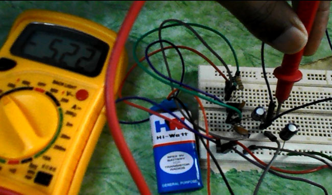
In electronics applications sometimes we need negative voltage. However getting a negative supply source is not a reliable option, when it is needed for low current applications. For many electronic circuits which require low power, we cannot go for a negative voltage power source. For the applications of reference or low power purposes one can go for circuits which can generate negative voltage from positive voltage supply.
There are many circuits for this purpose. Here we have designed a simple negative voltage generator circuit. This circuit is developed from 555IC timer circuit.
Components
+5 to +9 supply voltage
555 IC
1KΩ, 10KΩ resistors
104 (100 nF), 223 (22 nF), 22µF capacitors (2 pieces)
IN4148 diodes (2 pieces)
Testing probes.
Circuit Diagram and Working Explanation
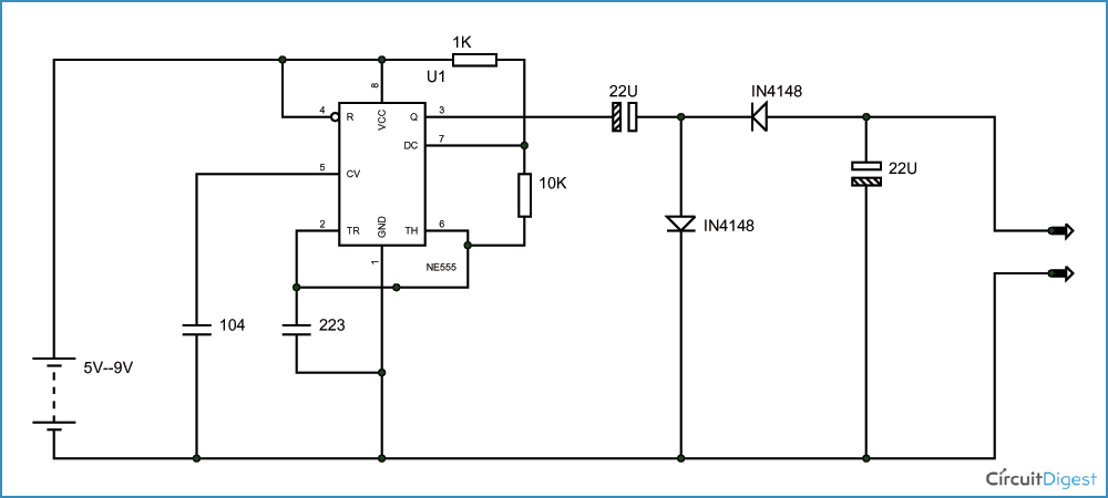
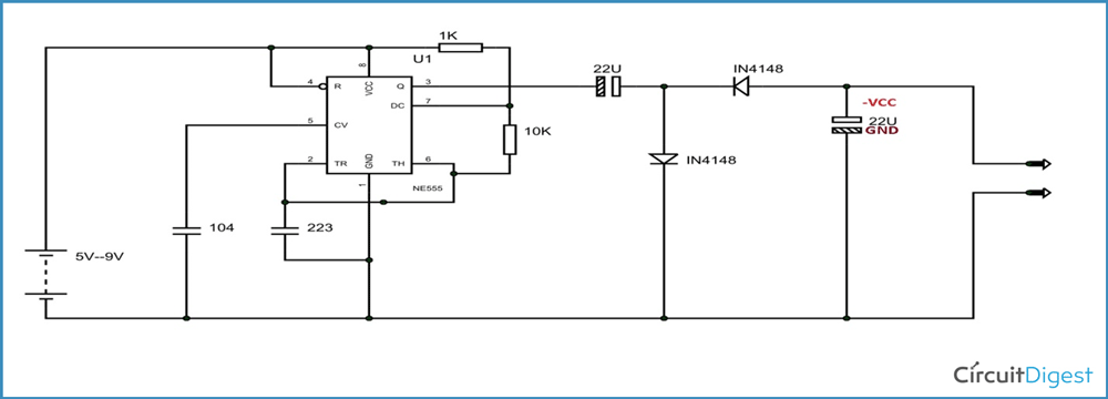
The above figure shows the circuit diagram of negative voltage generator. The 555IC timer here is acted as an ASTABLE vibrator. The capacitor here can be changed however the selection should pursued for maximum negative voltage. If selected capacitance does not suit well, than we can not get maximum negative voltage at the output.
As said earlier the 555 Timer IC acts as a square wave generator here and it generates square wave. The square will have a positive peak and +0 ground forming a complete cycle.
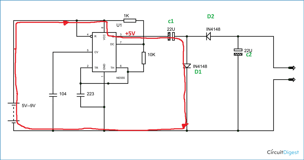
Now when there is a positive voltage peak at the output, there will be a current flow (REDLINE) as shown in figure below. During this time, the diode D1 will be forward biased and the diode D2 will reverse biased.
Because of this the capacitor C1 gets charged as shown in figure, and a voltage VCC appears across it.
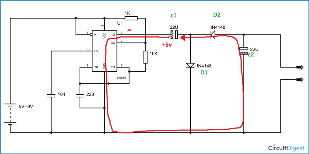
Now when ground appears after positive peak, there will be a current flow (RED LINE) as shown in figure below. During this time diode D1 will be reverse biased and diode D2 will be forward biased. With D2 being forward biased, the charge stored in capacitor C1 will have a way to flow. So the capacitor C1 discharges through D2, along the way it charges the capacitor C2. This is shown in figure.
So during 0V signal, there will a voltage appearing across C2 capacitor.
The voltage appeared across C2 will be of negative sign where referred to ground. This charging and discharging continuous with every cycle and there will be stable negative voltage across output with respect to ground.



Hello. I understand that there might be little chance to get some response considering that this is 7 years old article, but anyway. Maybe somebody else can answer:
Let's say that we have stable 5V input, like USB. Would it be possible to get regulated negative voltage like this: Using voltage divider between input (which is stable 5V) and output, we would create feedback voltage Vfb that could be referenced to required voltage Vref = 0V, or 0.7V? Then we would feed the Vfb to one of 555 pins that would enable/disable 555 like this Vfb<Vref --> disable astable vibrator; Vfb>=Vref --> enable astable vibrator. Perhaps this feedback could be fed to ¬RESET pin 4. Depending on where 555 actually resets (for LM555 typically 0.5V), this could be used to regulate the output voltage. Maybe properly oriented diode should be added between Vfb and GND to avoid negative voltage on pin 4, I don't know whether it matters or not.
Second, and I think an important question is how to calculate maximum current, that can be sinked by the output before the voltage drops significantly, assuming that input current is unlimited. Looking into datasheet of LM55 is not very promising, 1W would be absolute maximum dissipation for LM555. Could this perhaps be increased by adding external bipolar transisitor or mosfet and perhaps some reasonable inductor in series with D1?