As many of us know an Integrated Circuit or IC is a combination of many small circuits in a small package which together performs a task. Like an Operational Amplifier or 555 Timer IC is built by combination of many Transistors, Flip-Flops, Logic Gates and other combinational digital circuits. Similarly a Flip-Flop can be built by using a combination of Logic Gates and the Logic Gates itself can be built by using a few Transistors.
Logic Gates are the basics of many digital electronic circuits. From the basic Flip-Flops to Microcontrollers Logic gates form the underlying principle on how bits are stored and processed. They state the relation between every input and output of a system using an Arithmetic logic. There are many different types of logic gates and each of them has a different logic which be used for different purposes. But the focus of this article will be on the OR Gate because later we would be building an OR Gate using a BJT transistor circuit, similar to the AND Gate transistor circuit that we built earlier.
OR Logic Gates
OR gates implement Boolean ‘disjunction’, that is it helps in finding the maximum of the given binary inputs.
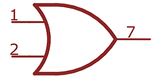
OR gates have the circuit symbol show in figure 1, the curved end is the input and the pointy end is the output. The logic they follow is simple, the output is true if any one input is true or if either input A or input B is true. The OR Gate Truth Table is shown below.
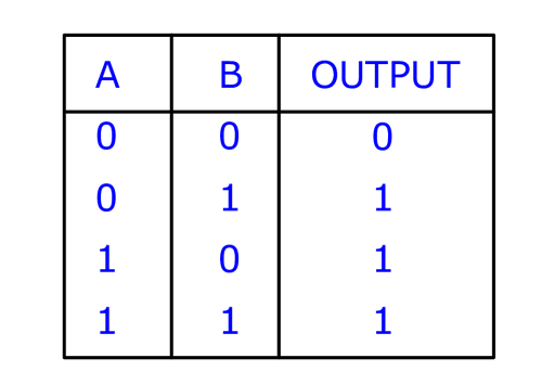
This principle can be extended to as many inputs as is needed, the output is true if any one (or at least one) of the inputs is true. In this article we will be building an OR Logic gate using transistor, if you want to know more on OR gate and how they work you can check this basics of OR gate article.
Parts Required
- NPN small signal transistors (2N2222, BC547, etc.)
- 1K resistors
- 10K resistors
OR Gate using Transistor – Circuit Diagram
The first version of the OR gate is the simplest one – it consists of two paralleled emitter followers sharing a common emitter resistor.
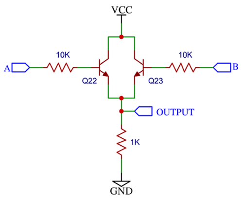
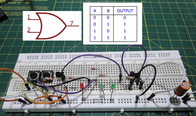
The above circuit diagram shows the simplest way to build an OR gate using NPN transistors. When input A is held high, a small current passes through the base of transistor Q22. This turns Q22 on, and (relatively) large current flows from the collector to the emitter. The current is dropped across the emitter resistor. The voltage across the emitter resistor is VCC – 0.7V, so the output ‘follows’ the input with a gain of a little less than unity. The same thing happens when input B is held high. When both the inputs are held high, both transistors are active, but the same voltage is dropped across the emitter resistor, and the output is still high. This circuit shows perfect OR behaviour. Connecting switches and LEDs to the input shows the behaviour of the circuit better as you can see in the below images.
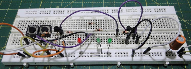
Case 1: When both the inputs are low, the output is low
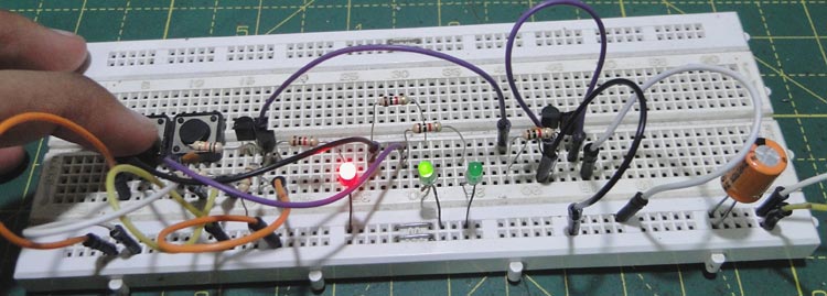
Case 2: When one input is low and the other is high, the output is high
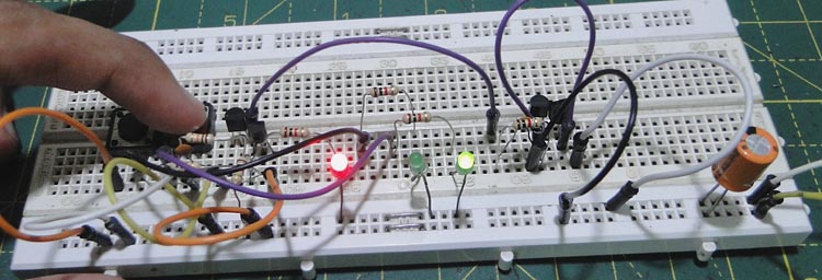
Case 3: And vice versa, when other input is low, the output is high
Case 4: And finally when both inputs are high, the output is high
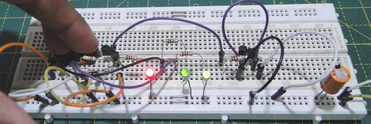
As you can see the circuit is working and following the truth table we discussed earlier. You can stop here if you are happy with this crude circuit, but if you want to make some improvements to the circuit read on.
OR Gate using Transistor – Improved version
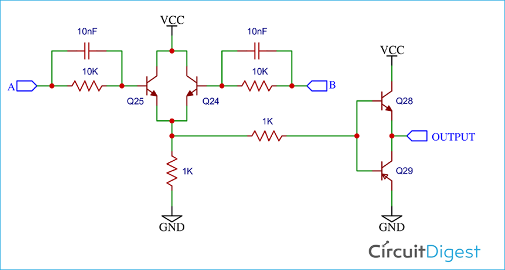
The circuit shown above was a very simple implementation of the OR gate, but this circuit is seldom used in the manufacture of ICs, for a few reasons. If we connect one input to VCC, a switch to the other input and probe the input and the switch and trigger on the rising edge of the switch, we notice a small problem.
The output goes high only after some time, i.e. does not respond instantly to the input. The time taken for the input to be seen at the output is called propagation delay. The same thing happens when the input is removed. The output takes some time to go back to ground.
This happens because of the transistor’s base capacitance. One solution would be to decrease the values of all the resistors, so that more current flows and the capacitances are charged quickly. But this would result in too much power dissipation. To circumvent this, we add two small (<10nF) ‘speedup’ capacitors across the base resistor to reduce the ‘storage’ time.
Another problem is that this circuit cannot sink as much current as it sources. Sourcing is not a problem because there’s at least one transistor turned on (when at least one input is high) that is connected directly to the output, so that the output can provide a decent amount of current.
However, when the transistor is turned off, only the 1K resistor pulls the output down, and sink current is limited. To make the drive symmetrical, an output push-pull stage is added. Both these modifications greatly reduce rising and falling propagation delays.
Applications of OR Gates
Along with the AND gate, the OR gate forms an integral part of all logic circuits. For example, if there are ten inputs that a microcontroller needs to monitor, a 10 input OR gate will tell the controller if any one of the inputs is high without needing ten input pins.
Another interesting applications of logical OR is in your car. The seatbelt warning light turns off only when all the doors are closed, in other words, if any one (or at least one) of the doors are open, the alarm lights up.



why use a PNP for the second set another NPN wouldn't it have worked?